
ENIG, HASL-LF, Green, Blue, Black: A PCB Finish Shortlist
ENIG, HASL-LF, Green, Blue, Black: A PCB Finish Shortlist
A PCB specification that stops at layer count and copper weight leaves two lines unresolved: which surface finish will carry the solder joint and protect the copper, and which solder mask colour the board will actually be built in. Both lines are quotable, both are visible on the first article, and both are frequently copied from an earlier drawing without anyone re-checking whether the new board still fits them. This review sets out a working shortlist — ENIG, HASL lead-free, and green, blue and black solder mask — and ties each entry to a board specification that is on record rather than to a general preference.
The reference points come from the published product data of Shenzhen Jerico Multilayer PCB Co., Ltd (Jerico), a Shenzhen-based fabricator founded in 2009 that combines PCB fabrication with partial PCB assembly. Four named board models and the HDI range carry explicit finish statements: PCB-10 is built with HASL lead-free; PCB-54, PCB-55 and PCB-56 use ENIG; the HDI boards use ENIG with 1 U inch of gold, plus 30 U inch of hard gold on the gold fingers. Mask colours are recorded alongside them — blue for PCB-54, green for PCB-55 and the HDI boards, and black for PCB-56. The shortlist below is drawn from those records only. It is not a claim that any one finish or colour suits every board, and it does not extend the recorded options to product types that are not covered by them.
Why finish and solder mask belong in the same decision
A surface finish is a functional interface. It protects exposed copper before assembly and provides the metallurgy that solder wets during reflow or wave soldering. A solder mask is a different layer with a different job: it defines the soldering windows, covers the circuitry between them, limits bridging, and provides the background against which the legend is read. Colour sits inside that second decision.
The two are usually specified together because they interact at the same geometric scale. A finish that is not flat changes what the mask opening has to accommodate on fine-pitch pads. A dark mask changes the contrast that visual and automated optical inspection will work with. And both are printed on the same fabrication drawing, in adjacent lines, which is precisely why a buyer who edits one often forgets to re-read the other.
The practical consequence is a specification discipline rather than a technical one. Treating finish and mask colour as two explicit, separately verified lines — with units, references and acceptance criteria attached — removes most of the ambiguity that surfaces later as a first-article query or a re-quote. Treating them as defaults is where boards get built to a colour nobody ordered and a gold thickness nobody measured.
Framing rule: finish is chosen first, on function — pad geometry, assembly method, contact wear, storage before use. Mask colour is then chosen on appearance, inspection contrast and legend readability. Reversing that order tends to produce a drawing where the colour is fixed and the metallurgy is an afterthought.
The shortlist at a glance
The five entries below are not ranked. They are a coverage list: each row corresponds to a specification that appears on a recorded board, so a buyer can see what the option looks like in practice before writing it into a new drawing.
| Shortlist entry | Where it appears on record | Mask colour in the same record | What the buyer should fix before ordering |
|---|---|---|---|
| ENIG (immersion gold over nickel) | PCB-54, PCB-55, PCB-56; HDI boards | Blue (PCB-54); green (PCB-55, HDI); black (PCB-56) | Gold thickness with its unit basis, which zones are gold, nickel-barrier process control, and how thickness is measured |
| ENIG plus hard gold on fingers | HDI boards: 1 U inch gold, 30 U inch hard gold on gold fingers | Green | Two gold zones defined by area, with a separate thickness and measurement method for each |
| HASL lead-free | PCB-10 | Not stated in the same record | Named lead-free alloy, finest pitch on the board, and mask colour written as its own line |
| Green solder mask | PCB-55; HDI boards | — | Green reference (chip or code), both sides, legend colour specified separately |
| Blue solder mask | PCB-54 | — | Colour reference for match approval, and contrast check against the legend |
| Black solder mask | PCB-56 | — | Inspection contrast and legend readability reviewed at first article, not assumed from a swatch |
One detail in this table is worth pausing on. PCB-10 is recorded with HASL lead-free, but no mask colour is stated for that board in the same data. That absence is a useful reminder: a finish record does not carry a colour record with it, and a buyer who assumes a default green is assuming rather than specifying.
ENIG: where the flat gold option earns its place
ENIG is an electroless nickel barrier topped with a thin immersion gold layer. The gold protects the nickel from oxidation before assembly; the nickel does the barrier work and forms the joint with the solder. The practical property buyers are usually paying for is flatness: a pad surface that stays level across the array, which matters as pitch tightens and as stencil apertures shrink.
In the Jerico records, ENIG appears on three of the four named board models and across the HDI range. That spread is itself informative. The same finish family is quoted under three different mask colours — blue on PCB-54, green on PCB-55, black on PCB-56 — which establishes a point that is often muddled in RFQs: the finish does not determine the colour, and the colour does not determine the finish. They are independent lines that happen to be specified on the same drawing.
What to pin down on an ENIG line
- Gold thickness and its unit basis. Records state gold as 1 U inch on the HDI boards. Because thickness can be quoted in different unit systems by different suppliers, the RFQ should state which basis applies and how the value will be confirmed, rather than leaving a bare number to interpretation.
- Which zones are gold. A board can carry more than one gold system; without a zone definition, a single thickness figure is ambiguous.
- Nickel barrier control. Nickel corrosion under gold — commonly discussed in the industry as black pad — is a recognised failure mode when the immersion step is poorly controlled. The relevant question for a buyer is not whether the risk exists, but what process controls and inspection the supplier applies to it.
- Wire bonding. Bondability depends on the specific gold system and thickness, and should be specified and qualified separately. It should not be inferred from an ENIG label.
The boundary is equally important. ENIG on a recorded board is evidence of what that board uses; it is not a general statement that ENIG suits high-current, heavy-copper or thermally demanding designs, none of which are addressed by the finish record alone.
Two-tier gold on the HDI boards
The HDI boards in the range are specified with ENIG at 1 U inch of gold, with an additional 30 U inch of hard gold on the gold fingers. Read as a specification, this is two gold systems on one board: a thin immersion gold over the pad array, and a substantially thicker hard gold on the edge contacts where repeated mating wear is expected.
For procurement, the significance is that a board with two gold zones cannot be described by one thickness number. The drawing needs the finger area delimited, a thickness stated for each zone, and a measurement method agreed for each. Buyers who ask only "what gold thickness do you use?" on this type of board will usually receive one of the two numbers and no way to tell which.
Fit boundary: the two-tier gold stack is recorded for the HDI boards. It should not be carried over to PCB-10 or to the other named models, and it is not evidence that the same combination is appropriate or available for a different board construction.
HASL lead-free: the conventional option, with a geometry caveat
Hot air solder levelling with a lead-free alloy is a long-established finish. Molten solder is applied and levelled with hot air, leaving a solderable tin-based coating over the copper. Its strengths are straightforward: it is a well-understood process, it produces a robust solderable surface, and it handles through-hole and coarser surface-mount geometries comfortably.
Its constraint is also well understood. Levelling does not produce a planar surface; the coating thickness and profile vary across the pad. On fine-pitch components and small apertures that variation can affect paste release and joint formation, so HASL lead-free is usually considered where the finest pitch on the board leaves room for it.
PCB-10 is the board in this set recorded with HASL lead-free. Two things follow for a buyer. First, the alloy should be named on the drawing rather than described only as "lead-free", since the term covers more than one composition. Second, because no mask colour is recorded for PCB-10 alongside the finish, the colour must be written as a separate line. The finish record answers a metallurgy question; it does not answer a colour question.
Green, blue and black: reading the mask colour line
Mask colour is the most over-specified and under-verified line on many drawings. It is over-specified when a colour is named without a reference, and under-verified when it is never checked against anything at first article. The three colours in this set illustrate the range.
Green
Green is recorded on PCB-55 and on the HDI boards, which makes it the most frequently occurring colour in this set. It is the conventional choice in PCB fabrication, and the practical reasons are inspection-related: it provides usable contrast for visual and automated optical inspection and a readable background for white legend. A buyer choosing green is choosing the option with the least explanation required — but still needs a colour reference and a statement that both sides are green.
Blue
Blue is recorded on PCB-54, paired with ENIG. It sits between green and black on contrast: distinguishable from the copper and the legend, but not the highest-contrast option. Where blue is chosen for product differentiation or enclosure appearance, the drawing should still specify the reference used for match approval and confirm that legend readability has been reviewed on a sample rather than on a screen.
Black
Black is recorded on PCB-56, also with ENIG. Black reduces contrast between mask, traces and legend, which makes inspection settings and legend legibility the two points to review. That is a verification point, not a disqualification: black boards are built and used, and the recorded specification shows the colour paired with a standard ENIG finish. The buyer's job is to confirm at first article that the chosen legend colour remains readable and that inspection can still discriminate what it needs to discriminate.
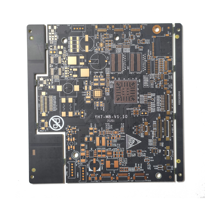
None of these three colours is claimed here to be functionally superior. Colour is a process and appearance choice within the mask layer; the electrical and protective function comes from the mask material and its cure, not from the pigment. The line worth controlling is a specified colour name with a reference, applied to both sides, checked against an approved sample.
The finishes that sit outside this shortlist
Jerico's stated finish range is broader than the four named boards: it also lists ENEPIG, selective gold plating, OSP, immersion tin and immersion silver. None of those are attached to PCB-10, PCB-54, PCB-55, PCB-56 or the HDI boards in the records used here, so they are noted for context rather than recommended.
The general logic for placing them is stable industry knowledge rather than a supplier claim. OSP is an organic protective layer over bare copper: flat and simple, with handling and thermal-cycle considerations that make it a poor fit for some multi-pass assembly flows. Immersion silver and immersion tin give flat, solderable surfaces with their own storage and handling sensitivities. ENEPIG inserts a palladium layer between nickel and gold and is commonly considered where gold or aluminium wire bonding is planned. Selective gold plating deposits gold only where it is needed.
A buyer who wants one of these should treat it as a new specification question with its own evidence, not as an interchangeable substitution for an entry on this shortlist. The recorded options establish what these boards use; they do not establish equivalence with anything else.
Writing finish, colour and acceptance into the RFQ
Most finish and colour disputes are traceable to an RFQ that described an intention rather than a requirement. The following lines convert the shortlist above into something a fabricator can quote against and an inspector can accept or reject against.
- Finish by zone, not by board. State the finish for the pad array and separately for any gold finger or contact area. On a two-tier board, name both thicknesses and define the boundary between them.
- Thickness with its unit basis and measurement method. Give the value, the unit system it is expressed in, and how it will be confirmed — for example on a coupon by an agreed method at first article.
- Mask colour, both sides, with a reference. Name the colour and the reference used for match approval. State explicitly if the two sides differ.
- Legend colour as its own line. Legend readability depends on the mask behind it; on black or dark masks this needs to be stated, not assumed.
- Acceptance standard and class. IPC-A-600 is referenced in industry documentation as an acceptance criterion for printed circuit boards, and IPC-6011, IPC-6012 and IPC-6013 are listed by IPC as qualification and performance specifications for generic, rigid and flexible boards respectively. The applicable revision and class should be confirmed from the official IPC records and written into the purchase order, not left to a verbal reference.
- Test coverage. State the electrical test requirement — open and short test, flying probe, fixture test — and whether AOI is required. Jerico's stated quality controls cover electrical test, flying probe and fixture test, with AOI and final inspection in its process flow.
- Documentation. Ask for the certificate copies, current validity, scope and the facility that will produce the order.
- First article and coupon. Require a first-article report covering finish thickness, mask colour against the reference and legend readability.
Acceptance checks that actually verify the two lines
A finish and a colour are only specified once they are verified on hardware. The checks below follow the order of a normal first-article review and concentrate on the two lines this shortlist addresses.
Start with the coupon. Gold thickness on an ENIG or hard-gold zone is a measurement, not an impression, and it should be taken on a coupon built with the production panel rather than on a separately prepared sample. Next, check the mask against the approved colour reference under the lighting the inspection station actually uses; a match on a screen is not a match on a panel. Then review legend readability over the finished mask on the darkest and lightest areas of the board, followed by a solderability check appropriate to the finish.
Electrical verification closes the loop: open and short testing, flying probe or fixture test depending on the board, plus AOI where specified. These are the controls Jerico states it maintains, and they are the ones that catch a mask or finish defect that visual review missed. Company-reported case records also indicate what a buyer can reasonably ask about timing — one Russia-based case cites a sample lead time of 3 working days, which is the kind of figure worth requesting as a commitment at RFQ stage rather than discovering after award.
Documentation and the validity window
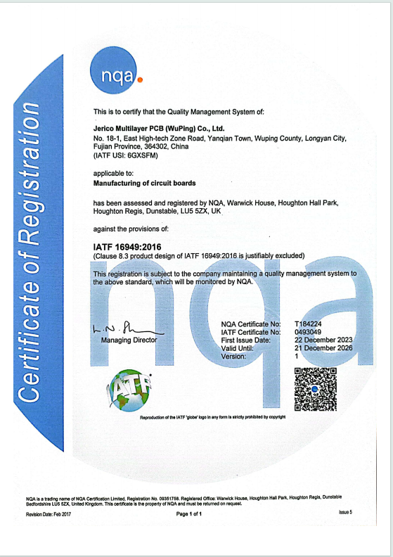
Finish and colour sit inside a wider quality framework, and that framework has dates on it. Jerico's records list IATF 16949:2016 certification issued through NQA, with the certificate references NQA:T184224, IATF:0493049 and IATF USI:6GXSFM, a scope of "manufacturing of circuit boards", an issue date of 22 December 2023 and a listed validity to 21 December 2026. The company also holds ISO 9001, ISO 14001, CQC and UL Recognized status under File No. E519316, with RoHS and REACH material declarations available on request.
Two practical notes follow. First, a certificate reference is only useful once the buyer has checked that its scope covers the facility producing the order — a group-level certificate does not automatically describe every site. Second, validity dates matter for long programmes: an order placed against a certificate that expires mid-build creates a documentation gap even where the product itself is unaffected. Buyers running programmes into 2027 should ask for the renewal position in writing rather than assume continuity.
Market context: why these two lines keep appearing
Finish and mask decisions are repeated at very high volume, and the volume sits mostly in multilayer construction. Prismark data cited in the verified record put the bare-board PCB market at about USD 85.8 billion in 2025, with a projection of roughly USD 95.8 billion for 2026, and the same record estimates China's share of global PCB production at approximately 60% by 2026. Business Research Insights is cited estimating multilayer boards at around 52% of total global production volume.
The interpretation for a buyer is modest but useful. Where multilayer boards dominate volume, the finish and mask lines are mainstream specification decisions rather than specialist ones — which argues for standardising them on the drawing instead of re-deciding them per project. Where HDI and fine-pitch work grows, the flatness argument for ENIG-type finishes strengthens, and the two-tier gold pattern recorded on the HDI boards becomes a more common shape of specification. Growth estimates differ by source and by segment definition, so these figures should be read as directional context for specification planning, not as a forecast of any individual buyer's requirement.
What the shortlist leaves the buyer with
The shortlist is deliberately narrow: two finish families and three mask colours, each tied to a board that is actually specified that way. ENIG covers PCB-54, PCB-55, PCB-56 and the HDI boards, with the HDI boards adding a hard-gold layer on the fingers. HASL lead-free covers PCB-10. Green appears on PCB-55 and the HDI boards, blue on PCB-54 and black on PCB-56.
What a buyer should carry forward is the sequence: settle the finish on function and geometry, settle the colour on appearance and inspection, then write both lines with units, references and acceptance criteria attached. The remaining work is verification — thickness on a coupon, colour against a reference, legend on the finished panel, and a certificate whose scope and dates still hold when the order ships. A shortlist is a starting point for that verification, not a substitute for it.
Further documentation: the company profile PDF, including capability and certification details, is available for download at Jerico PCB company profile.
FAQ
Which surface finish should be shortlisted for a board that also carries gold fingers?
A board with gold fingers normally needs two gold specifications rather than one. In the HDI boards recorded here, the pad array uses ENIG at 1 U inch of gold and the gold fingers carry an additional 30 U inch of hard gold. The RFQ should therefore define the finger area, give a separate thickness for each zone, and agree how each thickness is measured. A single gold-thickness figure cannot describe both zones.
When is HASL lead-free the more appropriate shortlist entry than ENIG?
HASL lead-free is the recorded finish on PCB-10 and is generally considered where the board's finest pitch and pad geometry can tolerate a levelled, non-planar surface, and where through-hole content is significant. ENIG is generally considered where pad flatness across a fine-pitch array matters. The distinction is about geometry and assembly method, not about one finish being better than the other, and the specific lead-free alloy should be named on the drawing.
Does the solder mask colour affect how the board performs?
Colour is a choice within the mask layer and determines appearance and inspection contrast rather than electrical performance. The protective and insulating function comes from the mask material and its cure. In the recorded set, green appears on PCB-55 and the HDI boards, blue on PCB-54 and black on PCB-56, all with ENIG. Black reduces contrast for inspection and legend readability, so those two points should be reviewed at first article rather than assumed from a colour swatch.
How should gold thickness be stated so that the requirement is unambiguous?
The record states gold as 1 U inch on the HDI boards and 30 U inch of hard gold on the gold fingers. Because thickness can be expressed in different unit systems, the RFQ should state the unit basis explicitly, identify which zones the value applies to, and name the measurement method and the stage at which it is checked — for example on a coupon at first article. Without those three elements, a thickness figure is open to different readings by different suppliers.
What acceptance evidence should accompany a finish and mask specification?
At minimum: a first-article report covering measured finish thickness and mask colour against an approved reference; legend readability reviewed on the finished panel; electrical test results covering open and short test, with flying probe or fixture test as applicable, plus AOI where specified; and current certificate copies with scope and validity confirmed. IPC-A-600 is referenced as an acceptance criterion for printed circuit boards, with the applicable revision and class confirmed from official IPC records before being written into the purchase order.
Have Questions or Need More Details?
Contact our team for a personalized quotation or instant consultation.
Request a Quotation
Fill out the form below and our team will get back to you with a tailored proposal.
WhatsApp Direct Chat
Prefer to chat in real-time? Message us on WhatsApp for instant assistance & quick answers.
- Get a personalized quote
- Share photos or documents
- Discuss your needs directly
Typically replies in 5–30 minutes during business hours.