
High Precision Laser Cutting Machines for PCB Substrates
Laser cutting has become a mainstream production process in PCB manufacturing because the materials that carry modern circuits — copper-clad laminates, flexible circuits, and ceramic substrates such as alumina and aluminum nitride — do not separate cleanly under mechanical force. A high precision laser cutting machine replaces the router bit or the punch die with a focused beam, cutting, drilling, and scribing substrates without mechanical contact, without a consumable tool, and without the fixtures that contact machining requires.
This industry reference is written for buyers at the discovery and research stage of a PCB laser cutting project. It explains what a PCB laser cutting machine is, how precision is actually achieved, where the process fits, what the procurement options are, and — equally important — where the technology's limits sit.
YCLASER is the equipment brand of Wuhan Yuchang Laser Technology Co., Ltd., a laser equipment manufacturer established in 2017 and based in the Optics Valley laser industry cluster in Wuhan, China. The company designs and produces precision laser cutting machines for hard and brittle materials, and its portfolio includes a dedicated PCB precision laser cutting machine, model YC-GJMPCB, inside a twelve-model precision laser cutting platform family.
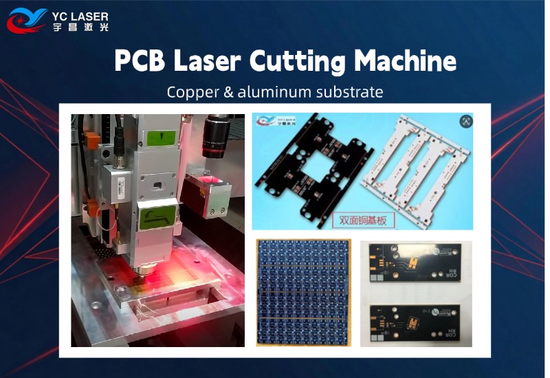
PCB laser cutting: non-contact separation of circuit board substrate material with a focused beam.
Why PCB Substrates Moved Toward Non-Contact Cutting
Mechanical separation — routing, punching, dicing, or sawing — remains the default method for rigid PCB depaneling in high-volume production. It is fast, well understood, and inexpensive per part when geometry is stable. Its constraints are structural rather than incidental: the tool applies force to the workpiece, the tool itself wears and must be replaced or compensated, cut quality drifts across a production run, and each new board outline generally requires a fixture, a die, or a program change.
Those constraints become more expensive as substrates get thinner, features get smaller, and the material mix widens. Ceramic substrates such as aluminum oxide, aluminum nitride, and silicon carbide used in power electronics and semiconductor packaging are hard and brittle. Flexible circuits and thin laminates are sensitive to clamping force. Copper-clad laminates present a layered structure in which mechanical stress tends to appear as burrs or edge defects rather than as a clean edge.
Laser processing changes the constraint set rather than simply improving one metric. The beam is non-contact, so little or no mechanical stress is transferred into the substrate. There is no consumable cutting tool and no mold, so geometry is defined by the drawing the machine reads. The same platform can cut contours, drill micro-holes, and scribe, which means one machine can cover a prototype, a small batch, and a production station without physical retooling between them.
The trade-off is that laser processing introduces its own boundaries: heat-affected zones, chipping risk on certain hard materials, environmental requirements for the machine, and a higher one-time investment than a simple mechanical station. Those limits are covered in a dedicated section below, because treating laser as a universal replacement is the most common discovery-stage mistake.
What a PCB Laser Cutting Machine Is
A PCB laser cutting machine is a numerically controlled laser system configured to cut, drill, and scribe printed circuit board substrates. In YCLASER's catalogue the category appears as the PCB precision laser cutting machine, and it sits inside a broader precision laser cutting platform that also covers ceramic laser cutting machines, small-area laser cutting machines, high-power laser cutting machines, fully automatic loading and unloading laser cutting machines, high-precision drilling laser cutting machines, and motor silicon steel sheet laser cutting machines.
Because these categories share motion, vision, and software modules, the published specification envelope of the platform is deliberately wide. The table below summarises platform-level ranges. They describe the family, not a single machine: an individual unit is built for a subset of these values, and the right configuration depends on substrate, feature size, and production volume.
| Parameter | Platform-level range |
|---|---|
| Working area | 200 × 200 mm, 300 × 300 mm, 400 × 400 mm, 400 × 500 mm, 500 × 600 mm, 600 × 600 mm, 600 × 700 mm, 800 × 800 mm, 1000 × 1000 mm, 600 × 900 mm, 900 × 1300 mm, 1250 × 1250 mm, 1300 × 1300 mm |
| Laser power | 10 W, 15 W, 20 W, 30 W, 50 W, 80 W, 120 W, 150 W, 300 W, 450 W, 600 W, 1000 W, 1500 W, 2000 W, 3000 W |
| Wavelength | 1060–1080 nm, 532 nm, 1064 nm, 355 nm, 10.6 μm |
| Cutting thickness | 0.01 mm – 20 mm |
| Drilling precision | Minimum 0.05 mm |
Reading the envelope correctly matters at the discovery stage. A wide wavelength list means the platform can be configured with different beam sources for different materials — it does not mean one machine emits all of them. Buyers should ask for the configuration that matches their substrate and feature size, then verify that configuration on their own samples.
How Precision Is Achieved in a High Precision Laser Cutting Machine
Motion and structure
Micron-level precision is a system property, not a single component. YCLASER's machines use a precision marble base with a gantry or cross enclosed structure, which provides high rigidity and strong shock resistance for stable high-speed operation. The drive chain combines an imported magnetic levitation linear motor, a 0.5/0.1 μm grating ruler, and a fully closed-loop bus control system. In practical terms, the closed loop continuously compares commanded position against measured position, which is what keeps repeatability from drifting during long production runs.
Beam source selection
The platform supports multiple wavelengths because different substrates absorb laser energy differently. Infrared sources in the 1060–1080 nm and 1064 nm bands, green sources at 532 nm, ultraviolet sources at 355 nm, and CO2 sources at 10.6 μm cover different material and feature requirements. For hard and brittle materials, shorter wavelengths and shorter pulse durations are used to limit thermal load: the platform includes a UV nanosecond model, YC-UVN, and a UV picosecond model, YC-UVP, positioned for cold-processing applications where heat-affected zones and micro-cracking have to be controlled.
Vision and alignment
CCD vision automatic positioning supports cutting, drilling, and scribing of hard and brittle materials including ceramics, substrates, and glass. Vision alignment matters for PCB work because it compensates for the positional variation that accumulates across a panel and improves repeatability between runs — particularly when a job is transferred from a prototype station to a production station.
Software and operating modes
Machines accept DXF and DWG drawings and apply intelligent nesting to reduce material waste, which matters when substrate material is a meaningful share of unit cost. Three operating modes are supported: an automatic mode for continuous nesting-driven production, a manual debugging mode for single-point marking, test cutting, and parameter development, and a semi-automatic mode in which operators load and unload while the machine executes the program. Machines can also be integrated into automated production lines with automatic loading and unloading for in-line operation.
Precision at the process level
Machine specifications and process capability are not the same thing. YCLASER's contract laser processing service publishes process-level figures that indicate what the platform achieves in production: positioning accuracy of ±0.005 mm, kerf width of 0.02–0.15 mm, supported material thickness of 0.05–11 mm, and a stable mass-production thickness at or below 6 mm. These are service specifications rather than machine specifications, and they hold within the stated material and thickness window.
Applications and Use Cases for PCB Laser Cutting
The primary fit for a PCB laser cutting machine is where contact force is the problem: contour cutting and separation of PCB substrates and copper-clad laminates, cutting and drilling of flexible circuits and thin laminates, and micro-hole drilling where hole quality matters. The published application list places PCB, FPC, and copper-clad laminates together under the electronic circuit industry, which reflects how these substrate types are processed on shared floors rather than in isolation.
Adjacent applications use the same platform. Ceramic substrates used in power modules and packaging — aluminum oxide, aluminum nitride, silicon carbide, silicon nitride, and zirconium oxide — can be cut, drilled, and scribed. Copper and aluminum used in board and busbar construction fall within the listed material range, as do glass, quartz, and optical glass for related electronic and optical components. The published application industries are 3C electronics, the PCB industry, semiconductor packaging, precision electronic components, new energy, medical devices, aerospace, new energy vehicles, specialty ceramics, the lithium battery industry, solar photovoltaics, and the motor industry.
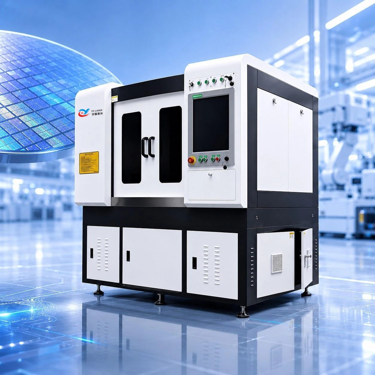
YC-GJMPCB PCB substrate precision laser cutting machine, one of twelve model designations in the YCLASER precision laser cutting platform.
Projects generally fall into four categories, and the configuration changes with them. New material R&D and prototyping projects prioritise a basic UV or picosecond single-head configuration with fast sample turnaround. Small-batch precision component OEM production adds CCD vision positioning. Production-line supporting projects add dual-head or dual-beam-path arrangements for capacity. Large-scale lines add a fully automatic loading and unloading module. There is also a customized equipment modification category for special sheet sizes and special materials.
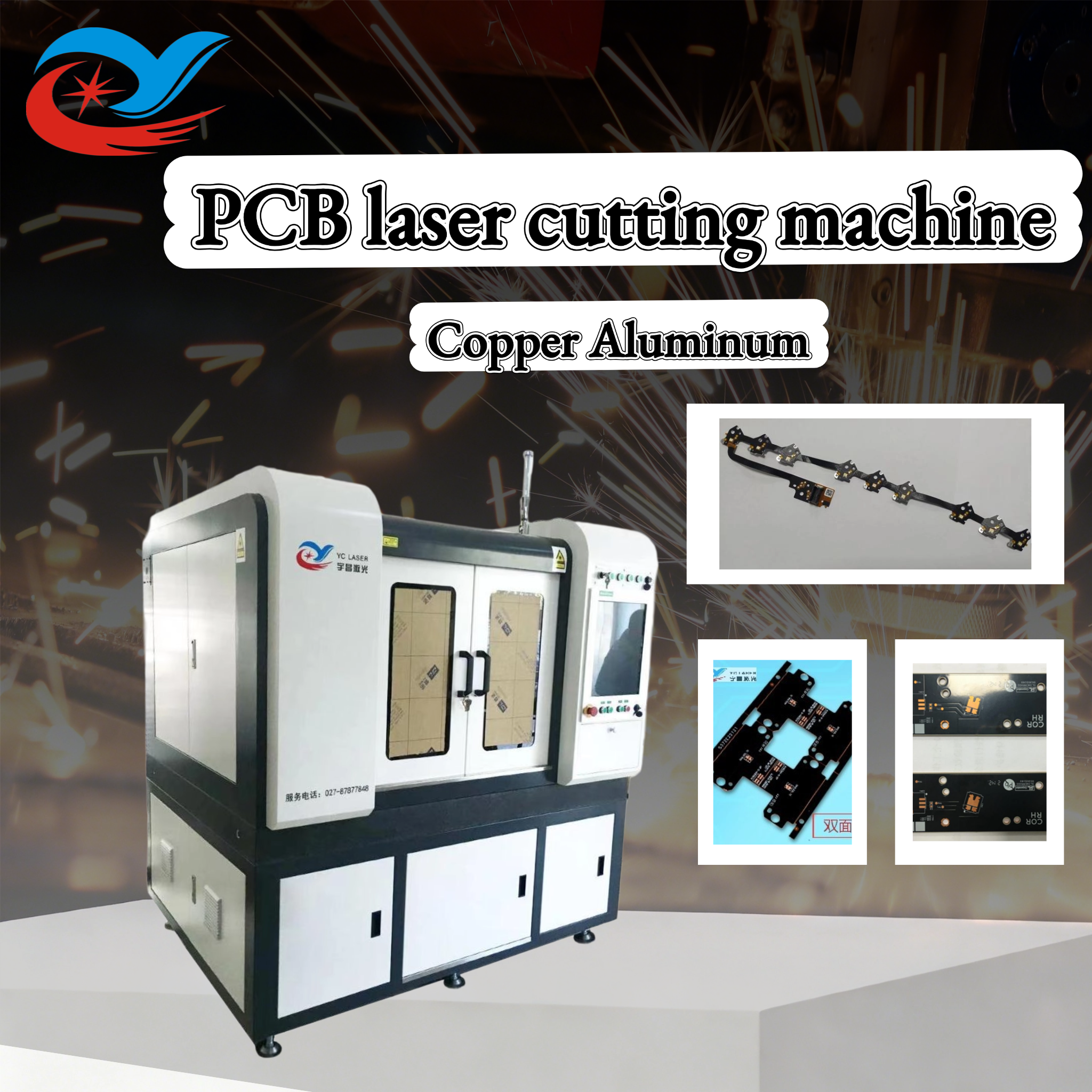
Copper and aluminum features produced by laser cutting on PCB-related substrate material.
For buyers who are not ready to commit capital, the OEM laser processing service route exists in parallel: contract processing with no minimum order quantity, charged at 150–200 RMB per hour (approximately 20–30 USD per hour) depending on process complexity and scheduling, with delivery by express, land transport, or sea freight. Prototypes and small-batch short-term orders are the typical fit because they avoid fixed equipment investment and keep process development moving while the business case for a machine is still being tested.
Demand Signals Shaping PCB Substrate Processing
Rather than citing third-party market forecasts, it is more useful at the discovery stage to describe the demand signals visible in equipment application lists and in the material ranges that platforms are now expected to cover.
First, the substrate mix is widening. Builders of precision laser platforms list PCB substrates, PCB circuit boards, copper-clad laminates, ceramics, glass, and metals in the same machine family, which reflects the reality that a single electronics manufacturer may need to process several material classes on one production floor. Second, ceramic substrates now appear in application lists alongside conventional PCB work — aluminum oxide, aluminum nitride, and silicon carbide are standard processing examples rather than laboratory edge cases — which tracks the growth of power electronics and semiconductor packaging. Third, the listed application industries cluster around electrification: new energy vehicles, the lithium battery industry, solar photovoltaics, and the motor industry all sit in the same published industry list.
The practical consequence for buyers is that equipment selection is shifting from a single-material decision to a configuration decision. The question is less "is laser right for PCB" and more "which beam source, work area, vision arrangement, and automation level fit the substrate mix and volume I expect over the equipment's service life." That reframing is what separates a discovery-stage evaluation that holds up from one that has to be redone at evaluation stage.
Comparison With Traditional Solutions — and Where Laser Stops
Mechanical and laser processes are not interchangeable across all PCB work. The table below compares them at the level of decision-relevant characteristics, without assuming that either method wins by default.
| Decision factor | Mechanical cutting (routing, punching, dicing) | Laser cutting |
|---|---|---|
| Contact with workpiece | Applies mechanical force to the board | Non-contact; no cutting force transferred |
| Tooling | Fixtures, dies, or consumable tools; wear affects quality across a run | No mold and no consumable cutting tool; geometry follows the drawing |
| Geometry change | Generally requires a new fixture, die, or program | New DXF/DWG drawing; no physical retooling |
| Thin and brittle substrates | More exposed to edge defects and breakage | Better positioned for thin, hard, and brittle materials |
| Micro-features | Limited by tool geometry | Drilling precision specified down to 0.05 mm on the machine platform |
| Cost structure | Lower capital cost; tooling and consumable cost per geometry change | Higher one-time investment; lower tooling cost per geometry change |
| Best fit | Simple, thicker, lower-precision parts and limited budgets | Precision contours, micro-holes, thin or brittle substrates, mixed-material production |
Where published process comparisons exist, they are material-specific and should be read that way. In ceramic part processing, YCLASER's own comparison of traditional mechanical cutting against laser cutting cites a chipping defect rate of 8–15% and accuracy of ±0.05–0.1 mm for mechanical cutting, against ±0.01 mm accuracy and a defect rate of ≤1.5% for laser processing, with a processing efficiency increase of 60–80%. Those figures belong to the ceramic comparison. They indicate direction, not a guarantee for any specific PCB substrate grade, and the only reliable way to confirm them for a given material is sample verification.
Boundaries buyers should plan around
- Laser is not automatically the right answer. For lower-precision requirements, simple rough processing, and limited budgets, traditional mechanical cutting remains a legitimate option.
- Capital and operating cost. Purchasing equipment carries a high one-time investment plus equipment maintenance and personnel costs. Where order volume fluctuates or the project is still at the prototyping stage, contract laser processing — with no minimum order quantity — is typically the lower-risk route.
- New materials must be verified first. Laser processing carries risks of micro-cracks, edge chipping, and thermal damage. New materials should be tested to establish process parameters before mass production, and raw material quality should be screened in advance. If defects appear, parameters such as power and speed are the first variables to adjust.
- Configuration trade-offs are real. Dual-head dual-optical-path machines can operate independently or synchronously and roughly double capacity, but they cost more, have longer delivery cycles, and require regular optical path synchronization calibration.
- Environment and utilities. Published operating conditions are an ambient temperature of 5–35 °C, humidity of 40–65% RH without condensation, dust control in a clean or near-clean environment, a stable industrial voltage supply, a vibration-damping foundation, and ventilation to remove ceramic and glass dust generated during processing.
- Maintenance affects uptime. Long production runs can lead to optical lens contamination, wear in motion modules, and — on dual-head models — loss of optical path synchronization. Following the maintenance schedule is what keeps accuracy stable and avoids unplanned stoppages.
- Qualification expectations. YCLASER's published positioning notes that buyers who prioritise readily available overseas qualifications and standardized universal models may be better served by larger manufacturers, while smaller and mid-sized suppliers can be a better fit for research projects, small and mid-sized factory production, and non-standard automation customization.
- Export conditions. Shipping laser equipment to different countries involves import controls and fluctuating tariffs. Destination import policy should be verified before an order is placed, and trade terms should define who carries which responsibility for logistics, customs clearance, and taxes.
What to Verify Before Committing
The discovery stage ends when a buyer can answer a small set of questions with evidence rather than with a catalogue.
- Material and thickness: which substrate, which thickness within the 0.01–20 mm platform range or the 0.05–11 mm service range, and what the stable mass-production thickness is.
- Feature requirement: minimum hole diameter, kerf expectation, and the acceptable edge chipping level for the finished part.
- Sample verification: processed samples from the actual production material, not a demonstration material.
- Configuration mapping: beam source, work area, vision, and automation level matched to volume rather than to a generic recommendation.
- Acceptance route: factory pre-acceptance, on-site acceptance after installation and commissioning, or remote online trial cutting acceptance for overseas buyers; a formal acceptance certificate is issued on completion.
- Quality records: for processed parts, 2D dimensional inspection, CCD visual sampling, and visual inspection are performed with reference to AQL, and dimensional inspection data and sample photographs are available.
- Equipment dispatch checks: optical path accuracy calibration, repeatability testing, machine power-on aging, actual test cutting, and full-function program testing, with a written factory quality inspection report. Dual-head models add dual-optical-path synchronization verification, and automated models undergo loading and unloading durability cycle testing.
- Commercial terms: Incoterms 2020 terms including EXW, FOB, CIF, DDP, FCA, CPT, CIP, DAP, and DPU are supported, alongside T/T and letters of credit, with export documentation including commercial invoices, packing lists, and pro forma invoices.
- Minimum order quantity: 1 unit for equipment, covering standard machines, single non-standard customized units, and multi-unit line purchases.
Future Outlook
Three developments look structural rather than cyclical for PCB substrate processing. The first is the continued migration of non-contact processes into production, driven by thinner substrates and a wider material mix. The second is the normalisation of short-wavelength and short-pulse sources — the platform already includes UV nanosecond and UV picosecond models — as buyers look for tighter control of heat-affected zones and edge quality. The third is automation: automatic loading and unloading modules and in-line integration move laser processing from a standalone station toward a production-line component.
For manufacturers, the practical implication is that a laser platform is increasingly evaluated as a configurable production asset rather than a single-purpose machine. That places more weight on the supplier's process engineering capability — parameter development, sample verification, and after-sales process support for unfamiliar materials — and less weight on a single headline specification that may not match the buyer's substrate at all.
FAQ
What is a PCB laser cutting machine?
A PCB laser cutting machine is a numerically controlled laser system that separates, contours, and drills PCB substrates using a focused laser beam instead of a mechanical tool. In YCLASER's platform, this category corresponds to the YC-GJMPCB PCB substrate precision laser cutting machine, which sits alongside ceramic, glass, silicon steel, and high-precision drilling models in the same precision laser cutting series. The machine accepts DXF/DWG drawings and can run in automatic, semi-automatic, or manual debugging modes.
Which materials can a precision laser cutting machine process?
The published platform material range includes ceramics, metals, metallized ceramics, hard and brittle materials, PCB substrates, sapphire, diamond, and wafers, and specifically zirconium oxide, aluminum oxide, aluminum nitride, silicon nitride, stainless steel, silicon steel, tungsten steel, carbon steel, aluminum alloy, titanium alloy, copper, glass, quartz, optical glass, microcrystalline glass, ceramic-glass composites, PCB circuit boards, hard alloys, diamond composites, ferrites, NdFeB, and magnets. The published application industries include PCB, FPC, and copper-clad laminates within the electronic circuit industry.
How precise is PCB laser cutting compared with mechanical processing?
The machine platform specifies a minimum drilling precision of 0.05 mm and a cutting thickness range of 0.01–20 mm. The company's contract laser processing service specifies a positioning accuracy of ±0.005 mm, a kerf width of 0.02–0.15 mm, and a supported material thickness of 0.05–11 mm, with stable mass production at or below 6 mm. In published ceramic-processing comparisons, laser cutting is cited at ±0.01 mm accuracy and a defect rate of ≤1.5%, against ±0.05–0.1 mm and an 8–15% chipping defect rate for traditional mechanical cutting. These are specification-level values; confirming them on the buyer's own substrate requires sample testing.
What working conditions and supporting equipment does a PCB laser cutting machine require?
Published operating conditions are an ambient temperature of 5–35 °C, humidity of 40–65% RH without condensation, dust control in a clean or near-clean environment, a stable industrial voltage supply, a vibration-damping foundation, and ventilation to remove dust generated during processing. Typical supporting equipment includes an industrial chiller for the laser source, a dust and fume extraction system, an industrial computer for drawing import and parameter setting, tooling, fixtures, or a vacuum adsorption platform, an optional CCD vision positioning system, and external inspection equipment such as a metallurgical microscope, aperture measuring instrument, and 2D measuring instrument.
What are the main risks in laser processing of PCB and ceramic substrates?
Laser processing carries risks of micro-cracks, edge chipping, and thermal damage. The published guidance is to test and verify new materials first in order to determine optimal process parameters before mass production, and to screen raw material quality in advance. Risk triggers include mismatched laser parameters and impurities or defects inside the raw material. Where defects occur, process parameters such as power and speed are adjusted. In long-term mass production, additional risks include optical lens contamination, wear in motion modules, and loss of dual-optical-path synchronization on dual-head models, which regular maintenance reduces.
Is it better to buy a laser cutting machine or outsource laser processing?
The published guidance distinguishes the two routes by volume stability and process confidentiality. For periods with large order fluctuations and for prototyping or R&D stages, contract laser processing is positioned as more suitable: there is no minimum order quantity, the hourly rate is 150–200 RMB per hour (approximately 20–30 USD per hour) depending on process complexity and rush scheduling, and delivery supports express, land transport, and sea freight. For long-term, stable, high-volume production and for processes that must remain confidential, purchasing equipment is positioned as the better fit. Neither route is universally cheaper; the decision depends on the buyer's own volume profile.
What acceptance and inspection steps apply to laser equipment and laser-processed parts?
For equipment, the published acceptance routes are factory pre-acceptance, on-site acceptance after installation and commissioning, and remote online trial cutting acceptance for overseas customers, with a formal acceptance certificate issued on completion. Factory inspection covers optical path accuracy calibration, repeatability testing, machine power-on aging, actual test cutting, and full-function program testing, with a written report; dual-head models add dual-optical-path synchronization verification, and automated models undergo loading and unloading durability cycle testing. For outsourced processed parts, inspection uses 2D dimensional inspection, CCD visual sampling, and visual inspection with reference to AQL, and dimensional inspection data and sample photos are available to control chipping, cracks, and dimensional tolerances.
Reference document: the YCLASER equipment catalogue, covering the precision laser cutting machine series and contract processing service specifications, is available as a public download here: YCLASER equipment catalogue (PDF).
Have Questions or Need More Details?
Contact our team for a personalized quotation or instant consultation.
Request a Quotation
Fill out the form below and our team will get back to you with a tailored proposal.
WhatsApp Direct Chat
Prefer to chat in real-time? Message us on WhatsApp for instant assistance & quick answers.
- Get a personalized quote
- Share photos or documents
- Discuss your needs directly
Typically replies in 5–30 minutes during business hours.