
Matching Process Materials to Fab Projects: A Semicera Guide
Industry context: Semiconductor process materials are the physical foundation of every fab step, from crystal growth to plasma etching. Choosing the wrong material can derail yield, uptime, and cost per wafer.
Problem / Opportunity
As device nodes shrink and wafer diameters grow, fabs face increasing demands on process materials: higher purity, extreme thermal stability, chemical resistance, and long-term reliability under harsh conditions. The global semiconductor materials market reached $67.5 billion in revenue in 2024, with wafer fabrication materials—including process chemicals and CVD materials—growing 3.3% to $42.9 billion. Within this ecosystem, components like SiC-coated graphite susceptors alone represent a ~$350 million market. Engineers and procurement teams must evaluate not just price, but the exact material properties required for their specific process module—epitaxy, annealing, etching, or diffusion—to avoid costly misalignment.
Brand Solution: Semicera’s Integrated Material Portfolio
Semicera (Ningbo Miami Advanced Material Technology Co., LTD) is a manufacturer of high-purity semiconductor process materials established in 2015, with a 40,000 m² factory and over 600 employees. The company produces more than 120,000 units annually across CVD SiC coating parts, CVD TaC coating parts, CVD PyC coating parts, SiC ceramic parts, semiconductor advanced ceramic parts, quartz parts, carbon fiber parts, and CFC materials. Its product line is designed to cover the four major thermal and plasma-based process categories: epitaxy, oxidation/diffusion, etching, and crystal growth.
Technical Explanation
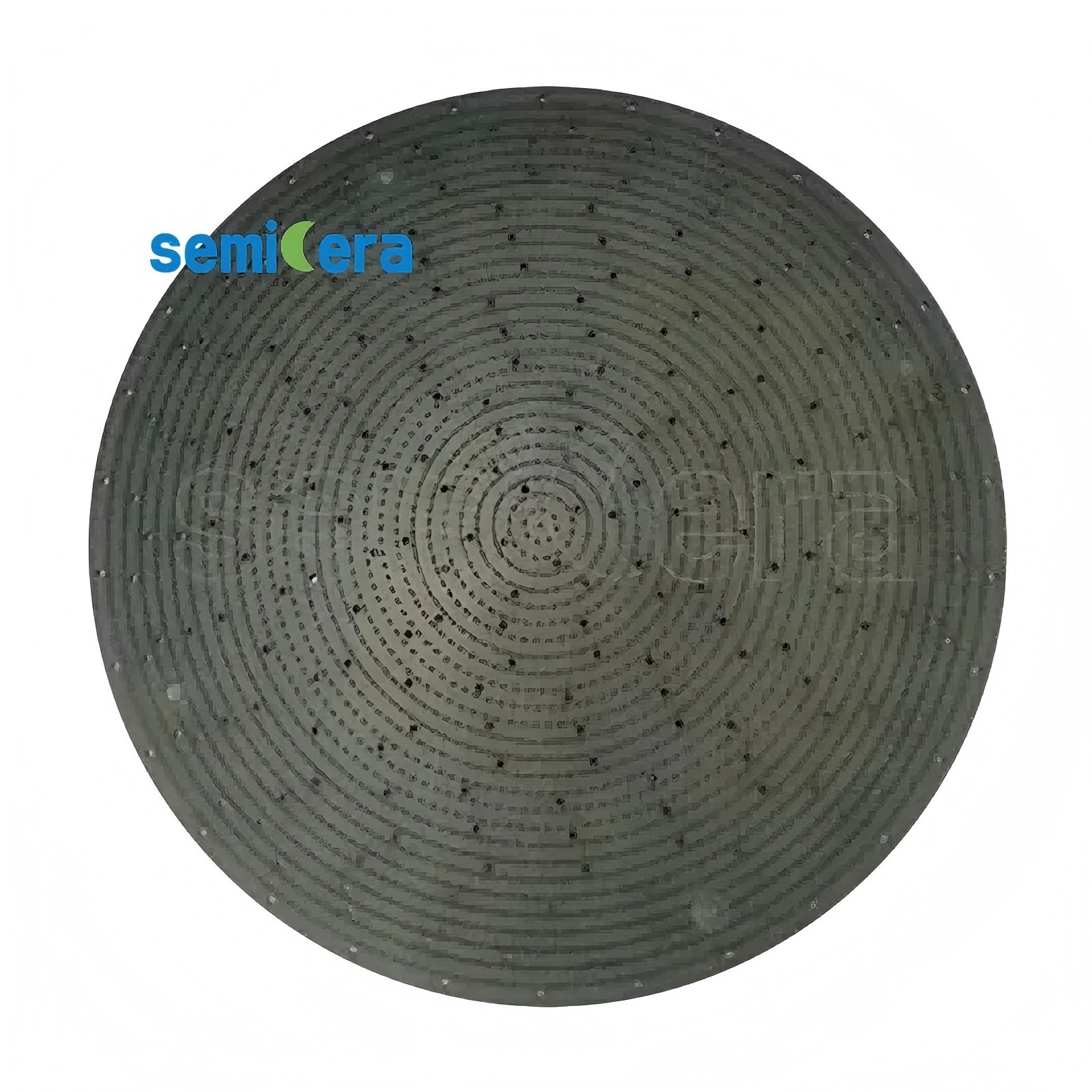
The core technology platform is chemical vapor deposition (CVD) coating on high-purity isostatic graphite substrates. Semicera’s CVD SiC coating achieves a purity level of 99.99995% (6N grade, total ash ≤5 ppm), a coating hardness of 2500 Vickers (40 GPa), and a FCC beta-phase polycrystalline (111) orientation. Typical coating thickness ranges 50–150 μm. For ultra-high-temperature epitaxy, CVD TaC coating (cubic tantalum carbide matrix) provides outstanding resistance to ammonia and hydrogen etching up to 2200°C. In etch applications, bulk solid CVD SiC parts—100% dense, zero porosity—deliver plasma erosion rates below 2 nm/min under CF₄/O₂ plasma. For diffusion and LPCVD processes, recrystallized or sintered SiC boats (e.g., model SiC-01) offer service lifespan >5× longer than traditional quartz boats while withstanding zero structural deformation at 1600°C.
Application / Use-Case Scenarios
Silicon Carbide Crystal Growth (Japan market): Semicera’s CVD SiC particles (model CVD-04, purity ≥99.9999%) serve as high-purity raw material for PVT furnaces. The ultra-low free carbon content (≤0.05 ppm) and consistent grain size (1.0–5.0 mm) improve crystal quality stability.
MOCVD Epitaxy (Asia-Pacific market): One Korea customer used 500 units per month of CVD SiC coated graphite carriers (CVD-01) and CVD TaC coated carriers (CVD-02) for GaN epitaxy. Result: edge ring replacement frequency reduced by 20%, with stable epitaxial layer quality over 2 years.
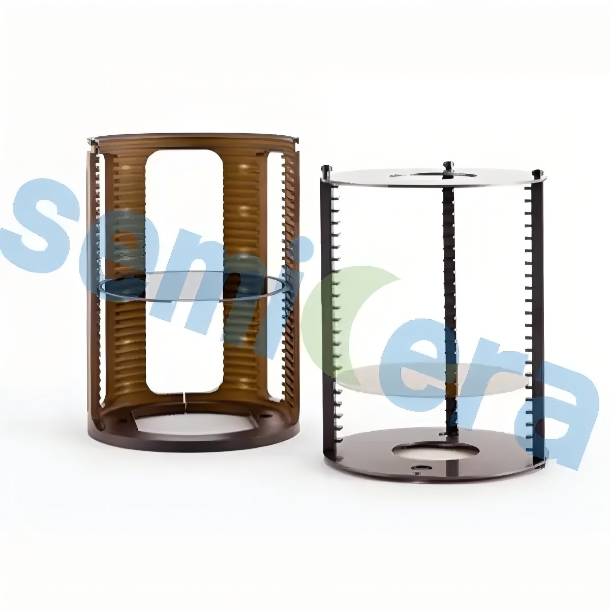
Oxidation/Diffusion (North America market): A US fab deployed 900 units per month of SiC wafer boats, SiC furnace tubes, and SiC paddles in LPCVD systems. The high-density CVD coating reduced equipment maintenance downtime by 15% and delivered consistent diffusion uniformity.
High-Temperature Insulation (Taiwan market): 1000 units per year of CFC material (carbon-carbon composite) were used in a silicon single crystal furnace. The 3D needle-punched matrix with tensile strength 90–140 MPa and ash ≤10 ppm improved energy efficiency and hot-zone temperature uniformity.
Market Trend Analysis
The global semiconductor graphite market reached approximately $1.62 billion in 2024, with a projected CAGR of 7.2% through 2032. Quartz fabricated parts for semiconductor manufacturing accounted for $2.21 billion in 2024, growing at 5.5% annually. TaC coatings are gaining traction for ultra-high-temperature SiC crystal growth; the top three suppliers held 99% of that niche market in 2022. CVD SiC coating remains the dominant protection method for graphite susceptors in MOCVD and epitaxial reactors. These figures underscore the transition toward more chemically resistant, high-purity materials driven by advanced packaging and wide-bandgap semiconductor demand.
Comparison with Traditional Solutions
Traditional quartz wafer boats and tubes offer lower initial cost but suffer from sagging, particle generation, and limited thermal shock resistance. Semicera’s SiC boats last up to 5× longer and operate at up to 1600°C without deformation. However, the upfront investment for SiC components is higher, and the supply of high-quality graphite blanks can be constrained during industry upcycles. For low-temperature processes that do not require extreme chemical resistance, advanced quartz or high-purity silicon still may be cost-effective alternatives.
Future Outlook
As GaN-on-SiC and SiC power device production scales, demand for ultra-pure TaC and SiC coated components will accelerate. Semicera’s vertically integrated production—from raw material purification to precision machining and CVD coating—positions it to address the next generation of process material requirements. The addition of advanced ceramic parts and continuous investment in R&D (100+ engineers) support customization for emerging fab designs, such as vertical batch furnaces and high-aspect-ratio plasma chambers.
FAQ
Which Semicera material is best for GaN epitaxy?
For GaN epitaxy using MOCVD tools, Semicera recommends CVD TaC coating graphite carriers (model CVD-02) with a TaC coating thickness of 25–45 μm. The cubic tantalum carbide matrix provides outstanding resistance to ammonia (NH₃) and hydrogen (H₂) etching up to 2200°C, preventing carbon contamination and ensuring epitaxial layer uniformity.
Can Semicera produce parts for etch processes using fluorine/chlorine plasma?
Yes. Semicera’s etch ring (model: Etch ring) is made from pure CVD solid SiC or high-purity silicon single crystal. It features a plasma erosion rate <2 nm/min under high-density CF₄/O₂ plasma, flatness tolerance ≤10 μm, and total metal purity <5 ppb, making it suitable for ICP-RIE and reactive ion etching systems.
What is the advantage of Semicera’s SiC wafer boat over quartz boats?
Semicera’s SiC-01 wafer boat (recrystallized/sintered SiC) offers a service lifespan >5× longer than traditional quartz boats, zero structural deformation at up to 1600°C, and excellent thermal shock resistance (1000°C to room temperature cycles). It is designed for high-temperature LPCVD and diffusion furnaces where quartz would sag and generate particles.
Does Semicera provide custom CNC machining for hot-zone components?
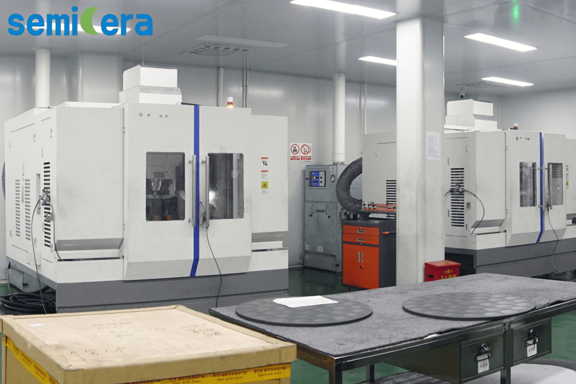
Yes. Semicera operates a 40,000 m² facility with more than 50 advanced production lines, including CNC graphite machining machines (see factory images). The company offers custom machining of high-purity isostatic graphite blocks (ash ≤5 ppm, grain size 2–5 μm) for heaters, susceptors, and crucibles, with typical lead time 30–50 days.
How does the purity of Semicera’s CVD SiC coating compare to industry standards?
Semicera’s CVD SiC coating achieves 99.99995% purity (6N grade, total ash ≤5 ppm), which meets or exceeds typical semiconductor requirements for epitaxial and RTP processes. The coating hardness reaches 2500 Vickers (40 GPa) and the crystal structure is FCC beta-phase polycrystal with (111) orientation, ensuring low particle generation and high thermal conductivity.
For a complete overview of Semicera’s semiconductor process material portfolio, download the product catalog: Semicera 2025 Catalog (PDF).