
PCBMASTER Factory Evidence: 6 In-House Plants, No Outsourcing
PCBMASTER Factory Evidence: 6 In-House Plants, No Outsourcing
Printed circuit boards are one of the few electronic components where a supplier's physical assets determine what is genuinely manufacturable. Yet a large share of the PCB supply market is asset-light: quoting platforms, trading companies and intermediaries that accept an order and place it into someone else's production line. For procurement teams working through the Decision and Execution stages of a complex program, that distinction is not cosmetic. It decides who owns the process, who can be audited, where a defect is caught, and how quickly a manufacturing problem can be diagnosed and corrected.
PCBMASTER is a China-headquartered, one-stop provider of PCB manufacturing and assembly (PCBA) services that launched as an independent brand in 2022 and is built on a founding team and core R&D engineers with more than 15 years of industry experience. The company operates six fully self-owned modern factories within an 80,000 m² manufacturing footprint, employs 700 people, maintains an engineering team of 100 engineers, and reports 100% export orientation, serving customers in the United States, Canada, Germany, the Netherlands, France, Poland, Hungary, the Czech Republic, Italy, Sweden, Denmark, Switzerland, the United Kingdom, Austria and Finland.
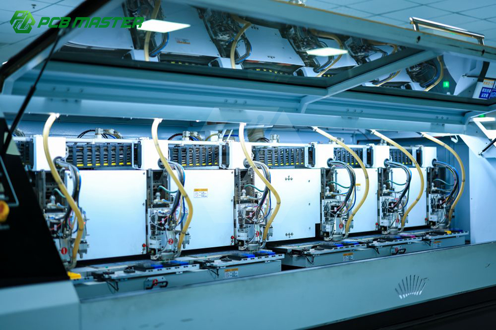
Drilling is executed on PCBMASTER's own lines rather than subcontracted, which keeps hole quality, registration and traceability inside one quality system.
Why Asset-Light PCB Supply Becomes a Problem at the Decision Stage
The commercial appeal of an intermediary model is easy to understand. Brokers and sales-only entities carry no plant overhead, quote quickly, and can appear to offer unlimited technology breadth because they route work to whichever factory is available. That flexibility is real, and for simple two-layer boards it is often adequate.
The problem appears when a program moves from quotation to execution. In an outsourced pooling model, the supplier of record is not the entity performing drilling, plating, lamination, imaging, routing or electrical test. When something goes wrong — a registration drift on a 14-layer stack-up, an impedance miss on a high-speed channel, a solder-mask defect on a fine-pitch area — the buyer's engineering team is separated from the process engineers who could explain it. Corrective action travels through a commercial layer before it reaches a machine. In practice this is where schedule risk, repeated rework and unclear accountability accumulate.
Asset-light sourcing is therefore not a defect in itself; it is a mismatch for programs where process control, data confidentiality and delivery continuity carry real cost. The practical question buyers are asked to answer is narrower: can the claimed capability be traced to equipment the supplier owns?
What “Six In-House Plants and Zero Outsourcing” Actually Means
PCBMASTER describes its manufacturing model as a closed-loop ecosystem: the full spectrum of its PCB output — rigid FR-4, high-layer-count boards, Any-Layer HDI, flexible circuits (FPC), Rigid-Flex, and specialty ceramic substrates such as AlN and Al₂O₃ — is produced inside its own facilities with no outsourcing. That is a manufacturing-structure claim rather than a marketing phrase, and it can be checked against a facility snapshot.
| Facility and capability snapshot | PCBMASTER (self-reported) |
|---|---|
| Brand status | Launched as an independent brand in 2022, built on a founding and engineering team with 15+ years of industry experience |
| Owned manufacturing plants | 6 fully self-owned modern factories |
| Manufacturing footprint | 80,000 m² |
| Workforce | 700 employees |
| Engineering team | 100 engineers |
| Annual output | 1,200,000,000 pcs |
| Export orientation | 100% export |
| Supply model | Closed-loop in-house production, zero outsourcing |
The Closed-Loop Process Chain
The value of plant ownership is best read as a process chain rather than a building count. PCBMASTER's own production documentation covers the sequence from bare-board fabrication through assembly, including drilling and post-drilling hole-position analysis; fully automatic circuit LDI (laser direct imaging) lines; DVCP vertical plating; automated laminating; solder-mask printing on a fully automatic line; legend marking; high-precision 6-axis routing; AOI electrical/optical inspection and fully automatic AVI visual inspection; flying-probe and fully automatic professional testing; and SMT assembly stages that include Yamaha pick-and-place, a 10-zone reflow oven, selective wave soldering, DIP insertion, and post/hand soldering.
Two consequences matter for buyers. First, process knowledge stays inside one organization: the engineer who reviews a stack-up can speak to the team that plates it. Second, the audit surface is finite. Instead of verifying an unknown set of subcontractors, a buyer verifies a defined set of lines and the quality system that governs them.
Engineering Review Before Metal Is Cut
PCBMASTER's risk documentation identifies the main failure modes it manages in-house: manufacturing defects in high-layer-count boards, material shortage and delivery delay in the supply chain, disclosure of customer Gerber files and hardware design data, layout-structure flaws, and mismatches between DFM rules and PCBA assembly processes. The stated control is a closed-loop digital DFM review in which an engineering group of more than 100 specialists checks every Gerber file before production, verifying parameters such as trace clearance and hole aspect ratio. For a procurement engineer, that step is the difference between a supplier who discovers a design conflict on the line and one who reports it before the first panel is processed.
The Technical Envelope That In-House Ownership Supports
Ownership of the process chain determines which technologies a supplier can quote with confidence. PCBMASTER's stated customization range covers 1–128 layer rigid FR-4, 1–32 layer FPC, Rigid-Flex, HDI, IC substrates, high-frequency materials, metal core and ceramic substrates. Its published standard parameter envelope documents the following boundaries.
| Parameter | Published envelope |
|---|---|
| Layer count (standard parameter envelope) | ≤ 64 layers |
| Any-Layer HDI stack-up | 12 layers |
| Stated technology range | 1–128 layer rigid FR-4; 1–32 layer FPC; Rigid-Flex; HDI; IC substrates; high-frequency materials; metal core; ceramic (AlN / Al₂O₃) |
| Maximum finished dimension | 620 × 1092 mm |
| Maximum finished board thickness | 4.2 mm |
| Differential impedance (>50 Ω) | ±7% |
| Single-ended 50 Ω impedance | ±6% |
| Layer registration tolerance | ≥3 mil (≤12 layers); ≥4 mil (>12 layers); ≥4 mil (N+N stack-up) |
| Pattern accuracy (board dimension >500 mm) | ±5 mil |
| Laser blind via | 65 / 165 μm |
| Max dimple of plated filled hole | 10 μm |
| Plating aspect ratio of through hole | 16:1 |
| Back-drill parameters | Min diameter 0.35 mm; min stub length 5 mil; min distance from back-drill to copper 5 mil |
| Supported special processes | POFV, N+N structure, hybrid lamination, deep blind microvia, metallized half hole |
| Materials | FR-4 TG180, FR-4 TG155, Rogers, PTFE, ceramics (AlN, Al₂O₃), polyimide (PI), metal-core (Al / Cu / Fe / Steel), BT and other IC substrate materials |
Read the range, then confirm the build. The 128-layer rigid FR-4 figure describes PCBMASTER's stated customization range for advanced programs, while the documented standard parameter envelope lists stack-ups up to 64 layers. The exact layer count, material set and tolerance combination for a specific design is confirmed during DFM review — owning a factory does not remove the need for engineering validation on either side.
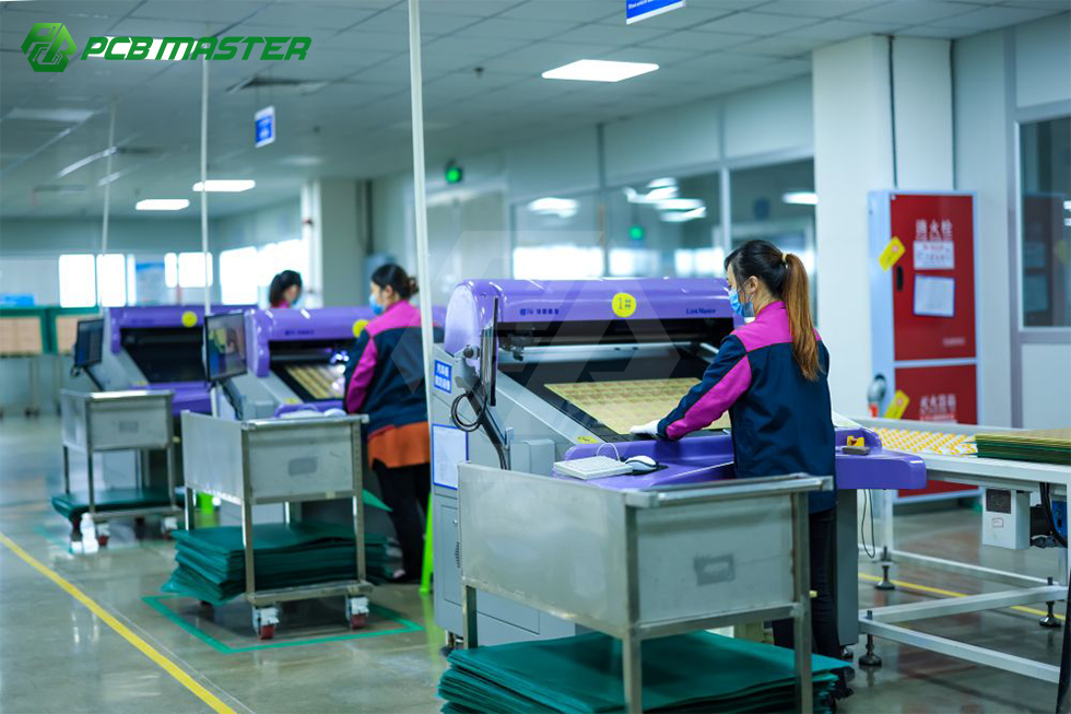
In-process AOI sits inside the same closed-loop facility as drilling, plating and imaging, so inspection data can be traced back to a specific process step.
Quality Control and Compliance Inside the Closed Loop
PCBMASTER states that quality control is performed in accordance with IPC Class 3 standards, the class intended for high-reliability products where continuous performance is critical. Final acceptance follows IPC-A-600 for bare-board acceptance thresholds and IPC-A-610 for assembly acceptability, with 100% final inspection producing complete flying-probe or bed-of-nails test logs, and structural RMA and after-sales tracking attached to the delivered lot.
Compliance is documented at the factory level rather than the sales level. PCBMASTER states that its production procedures comply with ISO 9001, automotive IATF 16949, UL safety certification and RoHS environmental directives, and that OEM services are provided for global markets. On the confidentiality side, legally binding NDAs are available for all projects, and customer PCB layouts and schematic drawings are circulated internally within the factories only, without external transmission to third parties. This matters for buyers in automotive, medical and AI-infrastructure programs, where design data is often more sensitive than the board itself.
PCBMASTER reports an in-house full-process defect rate below 0.85% and a 99.59% on-time delivery rate. These are first-party performance figures; a procurement team should treat them as claims to be tracked against agreed KPIs during the execution phase, not as externally audited statistics.
Applications That Depend on Factory Control
In-house ownership is most consequential where a board's failure mode is expensive or where qualification is slow. PCBMASTER lists its applicable industries as communications including 5G antenna PCBs, servers and data centers, automotive electronics, medical devices, industrial control, security, consumer electronics, and AI servers and other high-reliability or high-speed scenarios. The materials catalogue behind those applications — high-frequency laminates such as Rogers and PTFE, ceramic substrates including AlN and Al₂O₃, polyimide, metal-core (Al / Cu / Fe / Steel) and BT / IC substrate materials — is precisely the set that cannot be produced reliably through an unverified third-party pool.
The commercial structure complements the technical one. PCBMASTER operates with no minimum order quantity, starting from a single piece, which allows a laboratory prototype, a small-batch design iteration and a mass-production rollout to run through the same process definitions. Turnkey services combine full turnkey component sourcing, PCB fabrication, and flexible PCB assembly, so a development team can move from bare board to assembled unit without re-validating a new supplier at each step. Quick-turn boards ship within 24 hours, while FPC orders are delivered within 3–4 days. Shipping uses expedited global air express through carriers such as DHL and FedEx, with trade terms including DDP, and payment is compatible with PayPal, international credit cards and corporate wire transfer.
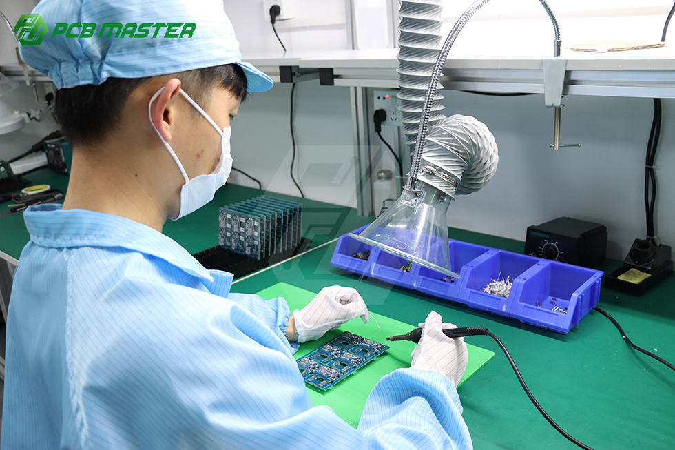
Post-soldering and hand-soldering under the same roof as fabrication allows assembly exceptions to be resolved with the fabrication team rather than a third party.
Market Trend: Why Verifiable Capacity Is Being Re-Priced
The demand backdrop explains why asset verification has moved up the procurement agenda. Prismark values the global PCB market at USD 73.6 billion in 2024, with a projection of USD 85.8 billion in 2025, driven by AI servers and high-speed networking. The AI server PCB segment is estimated by Goldman Sachs to grow from USD 3.1 billion in 2024 to USD 27.1 billion by 2027 — a segment whose stack-ups, layer counts and material requirements sit well outside commodity board production. Grand View Research estimates the flexible PCB market at USD 23.89 billion in 2024, with Asia Pacific holding a 76.8% revenue share, while Credence Research values the global Rigid-Flex PCB market at USD 25.4 billion in 2024 with a projected CAGR of 10.27% to USD 55.1 billion by 2032. Advanced IC substrates add a further layer of pressure: SNS Insider values that market at USD 19.23 billion in 2024 with a projected 15.69% CAGR through 2032.
Three implications follow for buyers. First, capability concentration: China accounted for 54% of global PCB production value in 2023 according to Prismark and CMB International, so most buyers will ultimately source from a region where the difference between real plants and sales entities is practically meaningful. Second, volatility in the specialty substrates that AI, medical and RF programs depend on, which rewards suppliers that hold materials and processes internally. Third, a benchmarking caution — global PCB market size estimates diverge between research houses depending on whether assembly services are included, so market figures should be treated as directional planning inputs rather than precise procurement baselines.
Comparing the In-House Model With Traditional Sourcing Models
Both sourcing models can be correct choices. The comparison below is structural, not a claim of universal superiority for either side.
| Dimension | Fully in-house, multi-plant model | Asset-light broker / multi-vendor pooling |
|---|---|---|
| Who performs fabrication | The supplier's own plants, across a closed-loop process chain | One or more third-party factories selected at order placement |
| Where defects surface | At in-house AOI, AVI, flying-probe and final inspection stages | After shipment to the intermediary's warehouse or the end customer |
| Corrective action speed | Directly with the process engineer who ran the step | Mediated commercially before reaching the machine |
| Design data exposure | Gerber files and schematics circulate internally under NDA only, per PCBMASTER | Depends on the data practices of each subcontractor involved |
| Capacity scaling | PCBMASTER reports 6–10 times the multilayer, HDI and rigid-flex order capacity of a single small workshop | Bounded by the availability of partner capacity at the time of order |
| Cost structure | Carries owned-plant overhead; advantageous for complex, high-mix work | Low overhead; often competitive on simple, standard boards |
Where the In-House Model Stops
An honest capability proof has to state its boundaries, and PCBMASTER's own documentation is explicit about several. Advanced PCB processes — HDI, rigid-flex, ceramic and high-frequency substrates — carry higher raw material and production costs than conventional FR-4 rigid boards, so an in-house supplier is not automatically the lowest-cost route for a straightforward board. Website pricing is reference-level; precise quotations depend on the detailed BOM, layer stack-up and special manufacturing requirements.
Physical constraints also apply. High-precision PCB manufacturing requires strict control of humidity, ESD and cleanroom cleanliness, plus a complete supporting supply chain and full-range test equipment — these are site-bound capabilities, not brand-level attributes. Published parameter limits such as a 0.35 mm minimum back-drill diameter, a 16:1 through-hole plating aspect ratio, a 620 × 1092 mm maximum finished dimension and a 4.2 mm maximum board thickness define what a given line can produce. Capacity is scheduled on demand rather than held as finished inventory, which should be factored into ramp planning. Separately, material and design choices such as metal-core or heavy-copper thermal structures can improve thermal management and power density, but specific efficiency metrics require design and thermal simulation verification rather than assumption.
Future Outlook
If AI server, high-speed networking and advanced substrate demand continue along the trajectories described above, the procurement dividing line will move from price per square meter toward verifiable process ownership. Buyers will increasingly ask for equipment-level evidence, process-level acceptance records and clear statements about what a factory cannot do. In that environment, suppliers with six owned plants and an internal test chain have an advantage that is documented rather than asserted, and suppliers without assets will need to compete on transparency instead of on breadth of claims.
For long-term programs, the more useful question is not whether a supplier is large, but whether the specific plants, lines and quality systems needed by a given product family will still be available — and auditable — in three to five years. Factory evidence is the starting point for that assessment, not the conclusion.
FAQ
What does “six in-house plants, zero outsourcing” mean for a PCB buyer?
It means the manufacturing steps required to produce and assemble a board — drilling, imaging, plating, lamination, solder mask, legend, routing, inspection, electrical test and assembly — are executed in facilities owned by the supplier rather than subcontracted. PCBMASTER states that rigid FR-4, high-layer-count boards, Any-Layer HDI, flexible circuits, Rigid-Flex, and ceramic substrates such as AlN and Al₂O₃ are all manufactured inside its own factories with no outsourcing, across six fully self-owned plants and an 80,000 m² footprint. For a buyer, the practical effect is that process ownership, inspection and final acceptance sit under a single quality system instead of being distributed across unverified subcontractors.
How can a procurement team verify factory ownership before awarding a project?
Verification typically proceeds in four steps: confirm the legal entity and site ownership rather than a mailing address; map the supplier's equipment list against the processes the design requires, such as LDI circuit patterning, DVCP vertical plating, AOI/AVI inspection and flying-probe testing; request process-level documentation including IPC-A-600 and IPC-A-610 acceptance records and test logs; and review the quality system certificates. PCBMASTER's production documentation covers its drilling, LDI, plating, laminating, solder-mask printing, legend marking, routing, AOI/AVI and electrical test stages, and the company states compliance with ISO 9001, IATF 16949, UL and RoHS. Each document should be verified project by project.
Does a fully in-house model limit which PCB technologies a supplier can deliver?
It can, if the factory set is narrow. PCBMASTER's stated service range covers 1–128 layer rigid FR-4, 1–32 layer FPC, Rigid-Flex, HDI, IC substrates, high-frequency materials, metal core and ceramic substrates, together with turnkey assembly. Its published standard parameter envelope documents stack-ups up to 64 layers, Any-Layer HDI at a 12-layer stack-up, finished dimensions up to 620 × 1092 mm, board thickness up to 4.2 mm, and a through-hole plating aspect ratio of 16:1. Layer count, materials and tolerances for a specific design are confirmed during DFM review rather than assumed from a headline range.
What are the practical limits of an in-house manufacturing model?
Three limits are worth planning around. Cost: advanced processes such as HDI, rigid-flex, ceramic and high-frequency substrates carry higher material and production costs than conventional FR-4 rigid boards, and precise quotations depend on the detailed BOM and layer stack-up. Environment and equipment: high-precision PCB manufacturing requires controlled humidity, ESD protection and cleanroom discipline plus matched inspection and reliability testing, which are site-bound rather than company-wide. Parameter bounds: features such as a 0.35 mm minimum back-drill diameter, a 16:1 plating aspect ratio or a 620 × 1092 mm maximum finished dimension define what a given line can produce, and monthly capacity is scheduled on demand.
How does factory ownership affect long-term supply continuity?
Continuity depends on capacity that can be re-allocated when demand or a design changes. PCBMASTER reports an in-house full-process defect rate below 0.85%, a 99.59% on-time delivery rate, quick-turn board shipment within 24 hours, FPC delivery within 3–4 days, and order capacity for multilayer, HDI and rigid-flex work 6–10 times larger than a single small workshop, operating with no minimum order quantity from a single piece. The company also uses legally binding NDAs and keeps customer layouts and schematics internal without transmission to third parties. These are first-party performance figures and should be tracked against agreed KPIs over the life of a program rather than treated as unconditional guarantees.
A technical profile document covering PCBMASTER's capabilities, manufacturing processes, parameter envelope and certifications is available for reference: PCBMASTER Profile (PDF).