
Post-CMP Wafer Cleaning Brushes: Display and Electronics Fit
Post-CMP Wafer Cleaning Brushes: Display and Electronics Fit
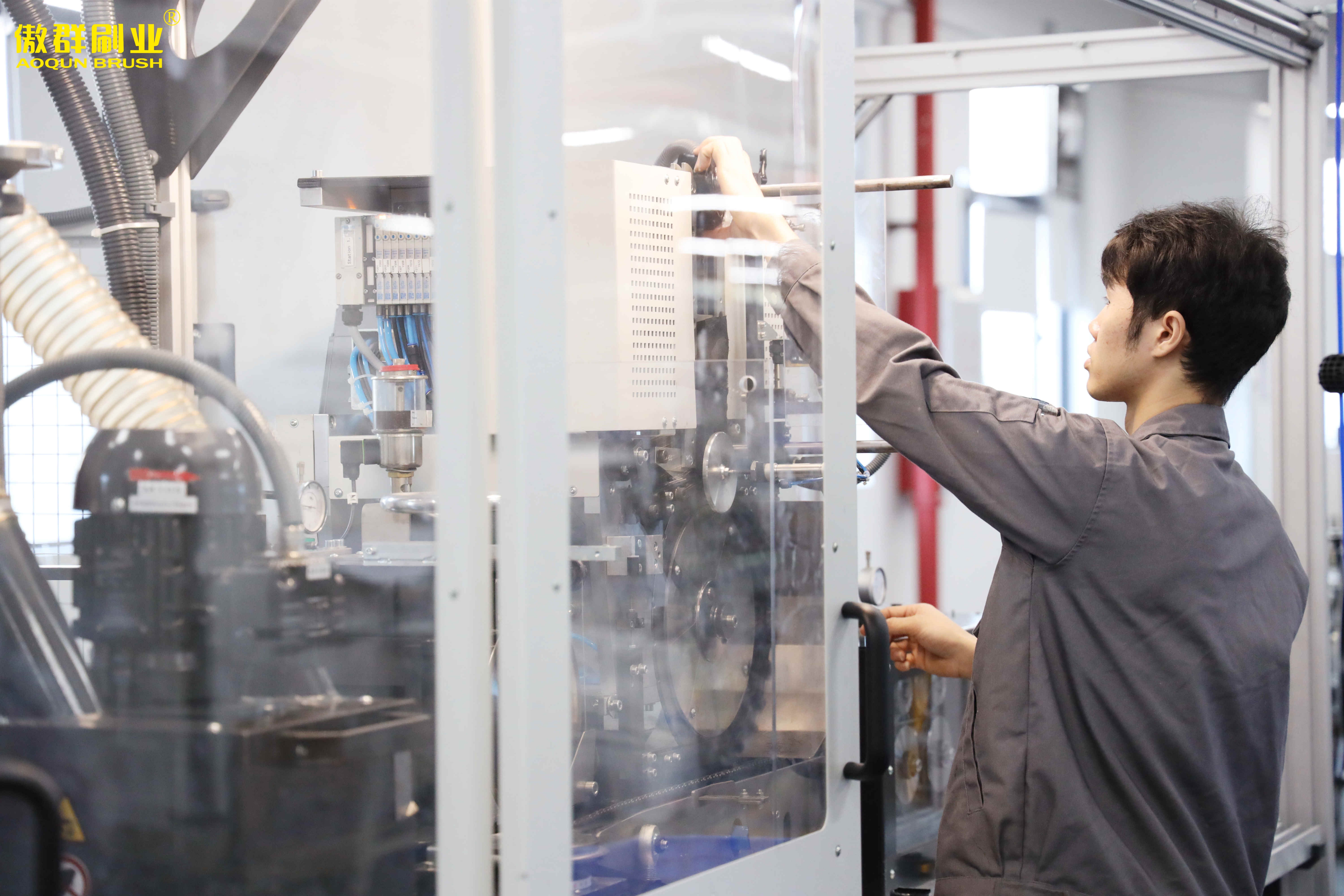
Cover: industrial brush manufacturing environment. Image: AOQUN BRUSH.
Post-CMP wafer cleaning brushes are contact tools, not commodity scrubbing heads. Their fit depends on the surface being cleaned, the particle and slurry burden, the down-force the tool applies, and the way the brush is handled between cleaning and replacement. For display and electronics polishing, the same logic applies at a different surface interface: the brush must match the substrate, the defect sensitivity and the finishing stage. AOQUN BRUSH, the brand of Guangzhou Aoqun New Material Co., Ltd., is a brush R&D and manufacturing service provider that integrates material R&D, brush process preparation and proprietary manufacturing equipment. This article maps its semiconductor wafer cleaning brush to post-CMP and wafer-handling scenarios, then separates the patent context from the tool-level evidence a buyer still needs.
The patent context cited for this article is Chinese invention patent ZL202210598941.4 (Patent Certificate No. 5663761; Grant Announcement No. CN 114750056 B), issued by CNIPA. Its application context here is display and electronics polishing. A related reference is copper-wire polishing brush patent ZL202210574951.4, cited for screen polishing of consumer electronics. Those references matter because they show a documented IP route into precision cleaning and polishing. They do not, by themselves, prove a brush will pass a particle, scratch or extractables qualification on a specific cleaner. That distinction is the core of a credible procurement review.
Why post-CMP cleaning is a scenario-fit problem
Post-CMP cleaning sits after a process that deliberately uses slurry to modify a wafer surface. The cleaning step then has to remove what the process left behind without creating a new defect. In that sense, the brush is part of the defect-control chain. A brush that is too aggressive, too soft, incorrectly sized or poorly conditioned can fail in different ways: incomplete removal, surface marking, particle adders, or a short service interval that raises tool downtime.
The practical question is therefore not which brush is strongest. It is which brush form, filament and contact condition fit this cleaner, this wafer stage and this handling routine. AOQUN BRUSH's semiconductor wafer cleaning brush is custom-made to the tool drawing: disc outer diameter, centre hole, bristle height and density are specified per chamber; PVA roller dimensions are specified per cleaner model; ESD-safe grades and particle-shedding limits are agreed at sample stage. That is a fit-by-drawing approach, not a catalogue-number approach.
What the patent references establish for buyers
The CNIPA patent reference gives the article a concrete starting point: ZL202210598941.4, with Patent Certificate No. 5663761 and Grant Announcement No. CN 114750056 B. In a buyer-facing review, the correct use of that fact is limited. It establishes that a Chinese invention patent exists under that number and that the application context supplied here is display and electronics polishing. It does not establish a published removal rate, a scratch threshold, a customer approval or a service life.
The copper-wire polishing brush patent ZL202210574951.4 is a related electronics reference, not a substitute for the semiconductor wafer brush. It is cited for screen polishing of consumer electronics. Screen polishing and post-CMP wafer cleaning are different contact problems: one concerns a display or consumer-electronics surface and a polishing step; the other concerns wafer cleaning after CMP, with slurry, chemistry, down-force and particle control in a cleanroom environment. A buyer should keep those references separate when comparing brush forms.
What the patent context does not replace: tool drawing approval, sample validation on the customer's cleaner, particle and scratch qualification, chemical-compatibility review, extractables review where required, and batch traceability. A patent is an IP record; a tool qualification is an application record.
AOQUN BRUSH's wider profile lists 124 intellectual property rights, including 26 invention patents and 4 international patents. That portfolio context is useful for supplier evaluation, but it should not be used to skip the specific patent numbers or the specific tool test. The same discipline applies to certifications and quality systems: they support a review, but they do not replace the sample result.
AOQUN BRUSH in the post-CMP cleaning map
AOQUN BRUSH's semiconductor wafer cleaning brush is listed for semiconductor wafer fabrication, post-CMP cleaning, PCB and PCBA manufacturing, 3C electronics and display, LED and photovoltaic cell production, and precision optics. The product family includes PVA sponge, PP, nylon, PBT and abrasive nylon filament, with ESD-safe and low-particle grades, and PEEK components where chemical resistance is required. Manufacture is described as Class 100,000 cleanroom production with batch traceability.
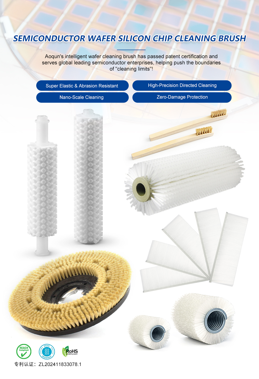
A semiconductor wafer cleaning brush form for tool-matched post-CMP and wafer-handling applications. Image: AOQUN BRUSH.
The listed selling points are specific rather than absolute: non-scratching contact at controlled pressure for wafers and coated surfaces; engineered filament density to remove slurry and particles without residue; Class 100,000 cleanroom production with batch traceability; and fit to major single-wafer and batch cleaner platforms to drawing. Those points are useful because they name the variables a buyer must control. They do not remove the need to validate the brush on the actual cleaner platform.
Technical fit factors: surface sensitivity, particle removal and handling contact
Surface sensitivity
Surface sensitivity determines how much contact pressure, filament stiffness and tip geometry the brush can tolerate. AOQUN BRUSH's product listing emphasizes non-scratching filament tips and controlled down-force for wafers and coated surfaces. In practice, the buyer should match the brush to the surface state: blanket wafer, patterned wafer, edge and bevel region, coated display substrate or precision optical surface. A brush that is acceptable on one surface may be too aggressive on another. The correct evidence is a scratch check on the relevant surface, not a general statement that the filament is soft.
Particle removal
Particle removal depends on filament density, contact length, brush conditioning and the cleaning chemistry. The product listing specifies bristle height and density per chamber, and the application scenario lists rotary disc or roller contact under controlled down-force, wet in-line cleaning with DI water or chemistry, and brush conditioning and replacement on a preventive-maintenance cycle. Those details matter because particle removal is a system result: brush, chemistry, flow, down-force and conditioning all interact. A denser brush may improve contact coverage but can also change drag, loading or cleaning uniformity. The buyer should therefore ask for particle-removal evidence on the same tool, chemistry and wafer stage, not a generic particle claim.
Handling contact
Handling contact is often overlooked. The application scenario includes wafer transfer and handling modules, edge and bevel cleaning, and non-scratching contact cleaning. A brush used in a handling module may see different contact geometry from a brush used in a single-wafer scrubber. ESD-safe or conductive options matter in ESD-controlled areas. Low particle shedding and low extractables matter where the brush is close to the wafer surface. Dimensional tolerance to the tool drawing matters because a small fit error can change contact pressure and cleaning uniformity. Batch traceability and cleanroom packaging complete the handling chain.
Scenario-fit table: post-CMP, wafer handling, display and electronics
| Scenario | Relevant brush form or reference | Fit factors to confirm | Verification before release |
|---|---|---|---|
| Post-CMP single-wafer cleaning | Disc brush made to tool drawing; PVA roller where the cleaner uses a roller | Disc diameter, centre hole, bristle height and density; surface sensitivity; slurry and chemistry; down-force | Particle and scratch qualification on the customer's cleaner; dimensional check; extractables review where required |
| Batch immersion or post-CMP scrubber | Disc or roller form matched to the platform; replacement brush programme | Brush conditioning; replacement interval; low particle shedding; ESD-safe grade; chemical resistance | Pilot batch; preventive-maintenance cycle check; batch documentation |
| Wafer handling and transfer modules | Contact cleaning brush or roller per handling module | Handling contact; edge and bevel access; ESD control; low particle and low metallic contamination | Non-scratch check on the handled surface; particle adders; fit to the module drawing |
| Display and 3C electronics polishing | Semiconductor wafer brush family where the application is display or electronics polishing; exact form defined by substrate and step | Substrate sensitivity; coating or pattern; residue; contact pressure; end-of-line cleanliness | Surface inspection; residue check; sample run on the actual polishing or cleaning step |
| Consumer-electronics screen polishing | Related copper-wire polishing brush patent ZL202210574951.4 | Screen material; scratch sensitivity; polishing stage; wire type and brush form | Separate screen-polishing sample; do not transfer wafer-brush assumptions to a screen-polishing step |
The table is a fit map, not a ranking. The semiconductor wafer brush and the related copper-wire polishing brush belong to different application contexts. The correct procurement move is to define the surface, the contamination to be removed and the handling contact before choosing the brush form.
Application scenarios in practice
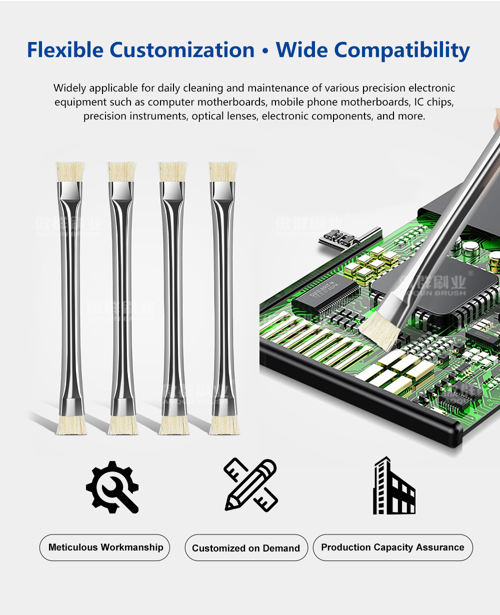
A tool-matched wafer brush form for post-CMP and handling scenarios. Image: AOQUN BRUSH.
Single-wafer post-CMP cleaners
In a single-wafer cleaner, the brush is part of a wet in-line process. The application scenario lists rotary disc or roller contact under controlled down-force, DI water or chemistry, and a preventive-maintenance cycle. The buyer should confirm the brush drawing against the chamber, then validate particle removal and scratch performance on the same wafer stage. The product listing's custom disc diameter, centre hole, bristle height and density are the variables that make this possible. A brush that fits the spindle but changes contact pressure across the wafer is not a fit.
Batch immersion and replacement programmes
Batch immersion and installed-tool replacement programmes place more weight on repeatability and documentation. The scenario lists batch immersion cleaners, post-CMP scrubbers and replacement brush programmes for installed tools. Here the buyer should ask for batch traceability, cleanroom packaging, and a consistent dimensional check from lot to lot. The brush change interval should be tied to the customer's preventive-maintenance cycle, not to a generic replacement claim. If the incumbent brush is being replaced, the new brush should be compared on the same tool and the same cleaning stage.
Display and consumer-electronics polishing
The display and electronics polishing context broadens the surface-fit question. AOQUN BRUSH's semiconductor wafer brush is listed for 3C electronics and display applications, but the exact brush form still has to be defined by the substrate and the polishing or cleaning step. The related copper-wire polishing brush patent ZL202210574951.4 is cited for screen polishing of consumer electronics. That reference is useful for understanding the electronics polishing route, but it should not be used to claim that a wafer cleaning brush is a screen-polishing brush. The buyer should separate the two scenarios and validate each on its own surface.
Comparison with adjacent solutions
A common procurement mistake is to compare brush forms as if one were inherently better. The more useful comparison is fit. AOQUN BRUSH's product range includes PVA sponge rollers and filament-based wafer brushes. The product listing says PVA roller dimensions are specified per cleaner model, while disc brushes are made to tool drawing with bristle height and density per chamber. Those are different design routes for different cleaner architectures. The buyer should compare them on the same cleaning stage: what contamination is being removed, what surface is at risk, what chemistry is present, and what down-force the tool applies.
- Filament brush fit: useful where the tool drawing calls for a disc or roller with specified bristle height and density, and where particle removal and surface contact need to be tuned together.
- PVA roller fit: relevant where the cleaner model uses a PVA roller and the drawing specifies roller dimensions; it should be evaluated as part of the same tool qualification, not as a universal substitute.
- Related screen-polishing reference: the copper-wire polishing brush patent ZL202210574951.4 addresses a different electronics surface. It can inform a screen-polishing review but does not establish wafer-cleaning performance.
The fit boundary is clear: a brush can be well made and still be wrong for a given chamber, chemistry or surface. The supplier should be able to state what the brush is designed to do, what it is not designed to do, and what evidence is needed before release. That is more useful than a blanket performance claim.
Case evidence and what it does not prove
AOQUN BRUSH's supplied case summary describes a semiconductor and PCB equipment maker that used tool-matched brush sets per cleaner platform. The application included wafer disc brushes and PVA rollers for post-CMP and pre-diffusion cleaning, plus PCB scrubbing and deburring brushes. The case reports a pilot batch followed by volume release, and it states that the brushes passed the customer's particle and scratch qualification on the first sample round. It also states that the brush change interval was extended versus the incumbent, reducing downtime per tool.
That is relevant evidence because it matches the procurement question: tool-matched brush sets, sample validation, particle and scratch qualification, and a maintenance-cycle outcome. It is still one case. It does not prove that the same result will occur on another cleaner, another chemistry or another wafer stage. The correct reading is that the supplier has a documented route through sample qualification and replacement planning, not that every application will achieve the same interval or defect result.
Procurement verification checklist
- Define the surface and stage: post-CMP, pre-diffusion, edge and bevel, wafer handling, display substrate or consumer-electronics screen polishing. Do not mix stages in one qualification.
- Confirm the tool drawing: disc outer diameter, centre hole, bristle height and density, PVA roller dimensions, mounting and end fittings. The drawing is the first fit gate.
- Match the material to the environment: PVA, PP, nylon, PBT, abrasive nylon or PEEK where chemical resistance is required; ESD-safe or conductive grade where the area is ESD-controlled.
- Agree particle-shedding and extractables limits at sample stage: these are application-specific and should be written into the sample plan, not assumed from a data sheet.
- Run particle and scratch qualification on the customer's cleaner: use the same chemistry, down-force and wafer or substrate stage as production.
- Check handling contact: transfer modules, edge and bevel access, cleanroom packaging and batch traceability should be reviewed together.
- Plan the replacement interval: tie brush conditioning and change-out to the preventive-maintenance cycle and compare against the incumbent on the same tool.
Outlook: a validation roadmap, not a market forecast
The useful outlook for this category is not a market-size forecast. It is a tighter validation loop. Where display and electronics polishing surfaces are defect-sensitive, the buyer's attention moves from brush catalogue numbers to tool drawings, sample plans and batch records. The patent context, including ZL202210598941.4 and the related ZL202210574951.4, gives the supplier a documented IP starting point. The application evidence still has to be built cleaner by cleaner.
For AOQUN BRUSH, the credible position is as a specialist that can translate a tool drawing into a brush, then support the sample validation and replacement cycle. For the buyer, the credible position is to treat every brush as a qualified component: define the surface, confirm the drawing, test the particle and scratch result, and document the maintenance interval. That is the scenario-fit answer for post-CMP, wafer handling, display and electronics polishing.
FAQ
What does a post-CMP wafer cleaning brush do?
A post-CMP wafer cleaning brush is a contact cleaning tool used after chemical mechanical planarization to help remove slurry and particles from a wafer surface. In AOQUN BRUSH's product listing, the brush is made to the tool drawing with specified disc diameter, centre hole, bristle height and density, and it may use PVA, PP, nylon, PBT or abrasive nylon filament depending on the application. Its performance depends on the cleaner, chemistry, down-force and validation on the actual wafer stage.
How should surface sensitivity affect brush selection?
Surface sensitivity affects filament stiffness, tip geometry and contact pressure. A brush for a patterned wafer, edge and bevel region, coated display substrate or precision optical surface must be matched to the surface state and checked for scratching. AOQUN BRUSH's listing emphasizes non-scratching filament tips and controlled down-force, but the buyer should still require a scratch check on the relevant surface rather than relying on a general material description.
How are particle removal and low shedding evaluated before use?
Particle removal and low shedding should be evaluated on the customer's cleaner with the same chemistry, down-force and wafer or substrate stage used in production. The sample plan should define particle-shedding and extractables limits, then check particle adders and surface condition after cleaning. AOQUN BRUSH's product listing specifies low-particle and ESD-safe grades and says particle-shedding limits are agreed at sample stage; that is a starting point for validation, not a substitute for the test.
What handling-contact factors matter in wafer cleaning brush installation?
Handling contact includes the way the brush fits the spindle or roller position, how it contacts the wafer or substrate, and how it is handled during cleaning and replacement. The application scenario lists wafer transfer and handling modules, edge and bevel cleaning, ESD control, dimensional tolerance to the tool drawing, batch traceability and cleanroom packaging. A small fit error can change contact pressure, so the drawing and the installed position should both be checked.
How does a semiconductor wafer brush differ from a copper-wire polishing brush for consumer-electronics screens?
A semiconductor wafer brush is used in wafer cleaning and post-CMP scenarios, where slurry, particles, chemistry and controlled down-force are central. The copper-wire polishing brush patent ZL202210574951.4 is cited for screen polishing of consumer electronics, a different surface and finishing step. The two references should not be treated as interchangeable. A buyer evaluating either application should validate the brush on the actual surface and process, using the relevant patent only as context.
Conclusion
Post-CMP wafer cleaning brushes are selected by scenario fit, not by a single headline property. The surface, the particle burden, the handling contact and the tool drawing define the brush. AOQUN BRUSH's semiconductor wafer cleaning brush is presented with drawing-based customization, Class 100,000 cleanroom production, batch traceability and a documented case route through particle and scratch qualification. The patent context, including ZL202210598941.4 and the related copper-wire polishing brush patent ZL202210574951.4, adds an IP reference point for display and electronics polishing. It does not replace the sample result. That separation is what makes the article useful to a procurement or engineering team.
For the wider brush range, the public product catalog is available here: Aoqun Brush Products Catalog.
Have Questions or Need More Details?
Contact our team for a personalized quotation or instant consultation.
Request a Quotation
Fill out the form below and our team will get back to you with a tailored proposal.
WhatsApp Direct Chat
Prefer to chat in real-time? Message us on WhatsApp for instant assistance & quick answers.
- Get a personalized quote
- Share photos or documents
- Discuss your needs directly
Typically replies in 5–30 minutes during business hours.