
Project-Specific Semiconductor Process Materials: A Semicera Application Guide
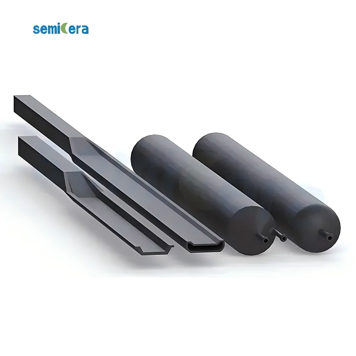
The complexity of modern semiconductor fabrication demands not only high-purity materials but also precise matching of material properties to specific process steps, temperatures, and gas chemistries. Semicera (Ningbo Miami Advanced Material Technology Co., Ltd), an integrated manufacturer of semiconductor process materials headquartered in Ningbo, China, addresses this challenge with a multi-material portfolio spanning coated graphite, advanced ceramics, quartz, and carbon-fiber composites. This article examines how Semicera’s product families align with distinct fab and substrate-manufacturing applications, offering a fact-based framework for process engineers and procurement teams evaluating materials for new or existing projects.
Market Context: Growing Demand for Specialized Process Materials
The global semiconductor materials market reached USD 67.5 billion in 2024, with wafer fabrication materials – including CVD chemicals and coated components – rising 3.3% to USD 42.9 billion (SEMI). Within this segment, semiconductor-grade graphite alone was valued at approximately USD 1.62 billion in 2024, projected to grow at a CAGR of 7.2% through 2032 (Verified Market Reports). Semicera dedicates 600+ employees and a 40,000 m² facility to produce more than 120,000 units annually, with over 100 engineers focused on R&D for advanced coatings and precision machining.
Material Portfolio and Process Coverage
Semicera’s catalog covers seven major material categories, each designed for specific thermal, chemical, or mechanical regimes encountered in semiconductor manufacturing:
- SiC-coated graphite carriers (model CVD-01) – FCC β-SiC coating, typical 100 µm, hardness 2500 HV, purity 99.99995% (6N). Used in MOCVD and RTP susceptors.
- TaC-coated graphite carriers (model CVD-02) – Cubic TaC coating 25–45 µm, operable up to 2200 °C, exceptional resistance to NH₃/H₂ etching. Ideal for ultra-high temperature epitaxy.
- Pure CVD solid SiC parts (CVD-03) – Fully dense, porosity-free, thermal conductivity ≥150 W/m·K. Applied as etch rings and dummy wafers in plasma environments.
- CVD SiC particles (CVD-04) – 6N+ purity, grain size 1.0–5.0 mm, free carbon ≤0.05 ppm. Used as PVT crystal growth source material.
- High-purity isostatic graphite (Semiconductor graphite) – Ash ≤5 ppm, ultra-fine grain 2–5 µm, flexural strength 45–65 MPa. Machined into hot-zone structural components.
- Carbon-carbon composites (CFC material) – 2.5D/3D needle-punched, tensile 90–140 MPa, ash ≤10 ppm after halogen purification. Used for heaters, crucibles, and bolts in CZ/PVT furnaces.
- Quartz components – Fused quartz furnace tubes (OH <20 ppm) and wafer boats (GE214 grade, SiO₂ ≥99.99%), for oxidation/diffusion processes up to 1300 °C.
Technical Highlights: Coating Integrity and Purity
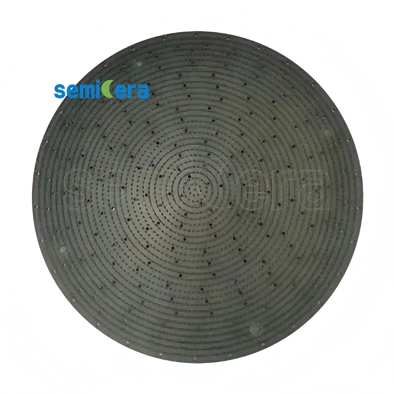
Semicera’s CVD SiC coating on graphite substrates achieves a Vickers hardness of 2500 HV (40 GPa) and a (111)-oriented β-phase polycrystalline structure. The coating thickness is held within ±10% of the target 100 µm. For TaC coatings, the cubic tantalum carbide matrix provides chemical stability against ammonia and hydrogen at 2200 °C, matching the coefficient of thermal expansion of the underlying graphite to prevent delamination. All carbon-fiber products undergo halogen purification to keep ash content below 10 ppm.
Application Scenarios: Matching Material to Process
Each Semicera product line is engineered for a defined set of operating conditions. The following table maps key use cases drawn from documented customer projects and application studies:
| Process Area | Recommended Product | Operating Conditions | Key Requirement |
|---|---|---|---|
| SiC crystal growth (PVT) | CVD SiC particles (CVD-04) | Ultra-pure vacuum induction >2000 °C | Total metals <1 ppm, free carbon ≤0.05 ppm |
| MOCVD / GaN epitaxy | TaC-coated graphite carrier (CVD-02) | 1600–2200 °C, NH₃/H₂ atmosphere | Zero carbon outgassing, CTE matched to graphite |
| Plasma etching (RIE) | CVD solid SiC etch ring (CVD-03) | High-density F/Cl plasma, RF-induced | Erosion rate <2 nm/min, metal <5 ppb, flatness ≤10 µm |
| Oxidation / diffusion (horizontal) | SiC wafer boat (SiC-01) | 1200–1600 °C, corrosive DCS/TCS | Zero deformation, lifespan >5× quartz boats |
| CZ / PVT hot zone insulation | CFC material (heater, crucible) | Up to 2500 °C, inert/vacuum | Tensile 90–140 MPa, ash ≤10 ppm |
In documented cases from Asia-Pacific and European fabs, Semicera’s components have demonstrated stable mass production over two years with reduced downtime and improved yield. For example, a Korean customer using TaC-coated carriers for epitaxy reported 20% fewer edge-ring replacements and consistent epitaxial layer quality.
Comparison with Conventional Solutions
Traditional quartz wafer boats in diffusion furnaces typically require replacement after 200–300 cycles due to deformation and particle generation. Semicera’s sintered SiC boats (model SiC-01) can withstand continuous operation above 1300 °C with a service life more than 5× longer than quartz, while maintaining slot-pitch tolerance of ±0.05 mm. However, the initial investment for SiC boats is higher than that for quartz, a trade-off that must be evaluated against total cost of ownership, particularly for high-throughput fabs running frequent batch processes.
Market Trends and Future Outlook
The increasing adoption of wide-bandgap semiconductors (SiC, GaN) drives demand for ultra-high-temperature compatible materials. The SiC-coated graphite susceptor market alone was estimated at USD 350 million in 2024 (Valuates Reports). Semicera’s ability to supply both CVD SiC and TaC coatings positions it to serve this growing segment. Additionally, the push for 300 mm wafer processing requires larger, more uniform process tubes and boats, which Semicera addresses with quartz furnace tubes up to 3000 mm and SiC furnace tubes with wall-thickness uniformity of ±0.2 mm.
Explore Semicera’s full product catalog and technical specifications: Download the 2025 brochure (PDF) or contact the team at sales05@semi-cera.com / WhatsApp: +86 15957878134. Visit www.semi-cera.com for more.