
Semicera OEM Semiconductor Process Materials: From Lab to Fab
The Growing Demand for Customized Semiconductor Process Materials
The global semiconductor materials market reached $67.5 billion in revenue in 2024, with wafer fabrication materials alone accounting for $42.9 billion. As chipmakers push toward smaller nodes, 3D architectures, and wide-bandgap substrates like silicon carbide, the process materials used in epitaxy, annealing, etching, and crystal growth must meet increasingly stringent purity, thermal, and dimensional requirements. Off-the-shelf components no longer suffice; fab engineers and equipment OEMs instead seek customized semiconductor process materials that can be tailored to specific reactor designs and process chemistries.
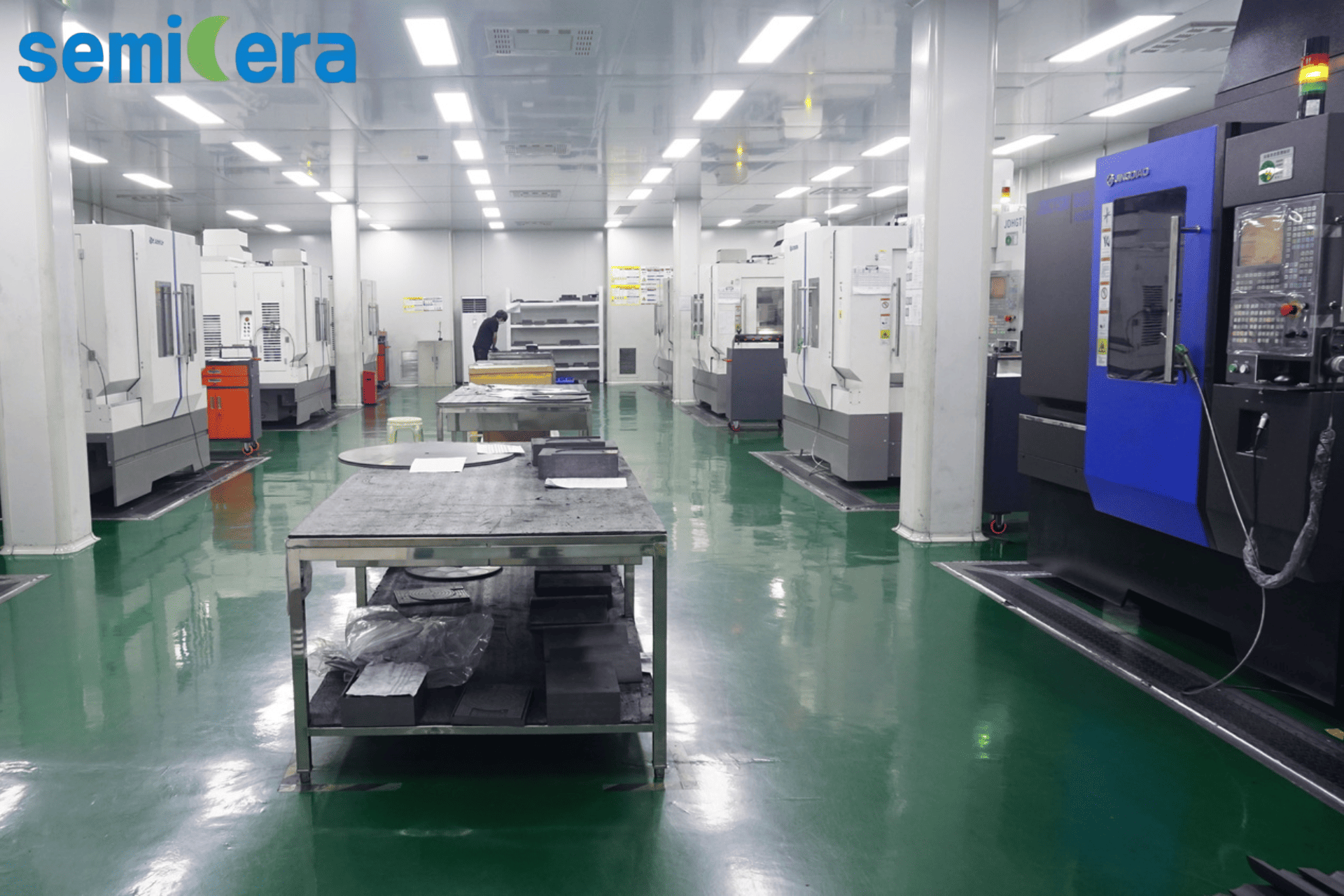
Problem: Off-the-Shelf Materials Limit Fab Performance
Standard hot-zone components often force process compromises. Graphite susceptors may lack the coating purity needed for ammonia-rich MOCVD environments; quartz boats warp under repeated thermal cycling; insulation felts shed particles. For high‑volume manufacturing of advanced logic, memory, or power devices, one-size-fits-all materials can lead to yield loss, unscheduled downtime, and higher cost of ownership. The industry needs suppliers that can engineer materials at the atomic scale while meeting OEM voltage, logo, and interface requirements.
Solution: Semicera’s Integrated OEM Capability
Semicera is a semiconductor materials and components manufacturer headquartered in Ningbo, China, that integrates R&D, production, and global sales under one roof. Since its founding in 2015, the company has grown to over 600 employees across three production bases covering 40,000 m², with an annual output exceeding 120,000 units. More than 100 engineers focus on advanced coating technologies, precision machining, and quality control. Semicera offers full OEM services, including customization of voltage and logo, with a minimum order quantity of just 1 unit and a typical lead time of 30–50 days. Monthly production capacity exceeds 10,000 units, enabling both prototyping and volume ramp.
Core Product Portfolio
- CVD SiC coated graphite carriers (model CVD-01) – coating thickness 50–150 µm, purity 99.99995% (6N), hardness 2500 Vickers, used in MOCVD and RTP epitaxy.
- CVD TaC coated graphite carriers (model CVD-02) – coating 25–45 µm, operating temperature up to 2200 °C, outstanding resistance to NH₃ and H₂ etching.
- CVD solid SiC parts (model CVD-03) – density ≥3.21 g/cm³, zero porosity, thermal conductivity ≥150 W/m·K, for SiC crystal growth.
- CVD SiC particles (model CVD-04) – 6N+ purity, grain size 1.0–5.0 mm, free carbon ≤0.05 ppm, for PVT SiC growth.
- Etch rings – plasma erosion rate <2 nm/min, flatness ≤10 µm, metal purity <5 ppb.
- Quartz boats and furnace tubes – GE214-grade fused quartz, SiO₂ ≥99.99%, working temperature up to 1150 °C continuous.
- SiC wafer boats (model SiC-01) – sintered or recrystallized SiC, max 1600 °C, lifespan >5× that of quartz.
- SiC furnace tubes and paddles – length up to 3000 mm, wall thickness uniformity ±0.2 mm, load capacity up to 15 kg at >1100 °C.
- Carbon fiber insulation – rigid and soft felt with ash content ≤5 ppm (ultra grade), processing temp up to 2500 °C.
- CFC materials – 2.5D/3D needle-punched composite, tensile strength 90–140 MPa, ash ≤10 ppm after purification.
- Semiconductor graphite – ultra-fine grain (2–5 µm), ash ≤5 ppm, flexural strength 45–65 MPa.
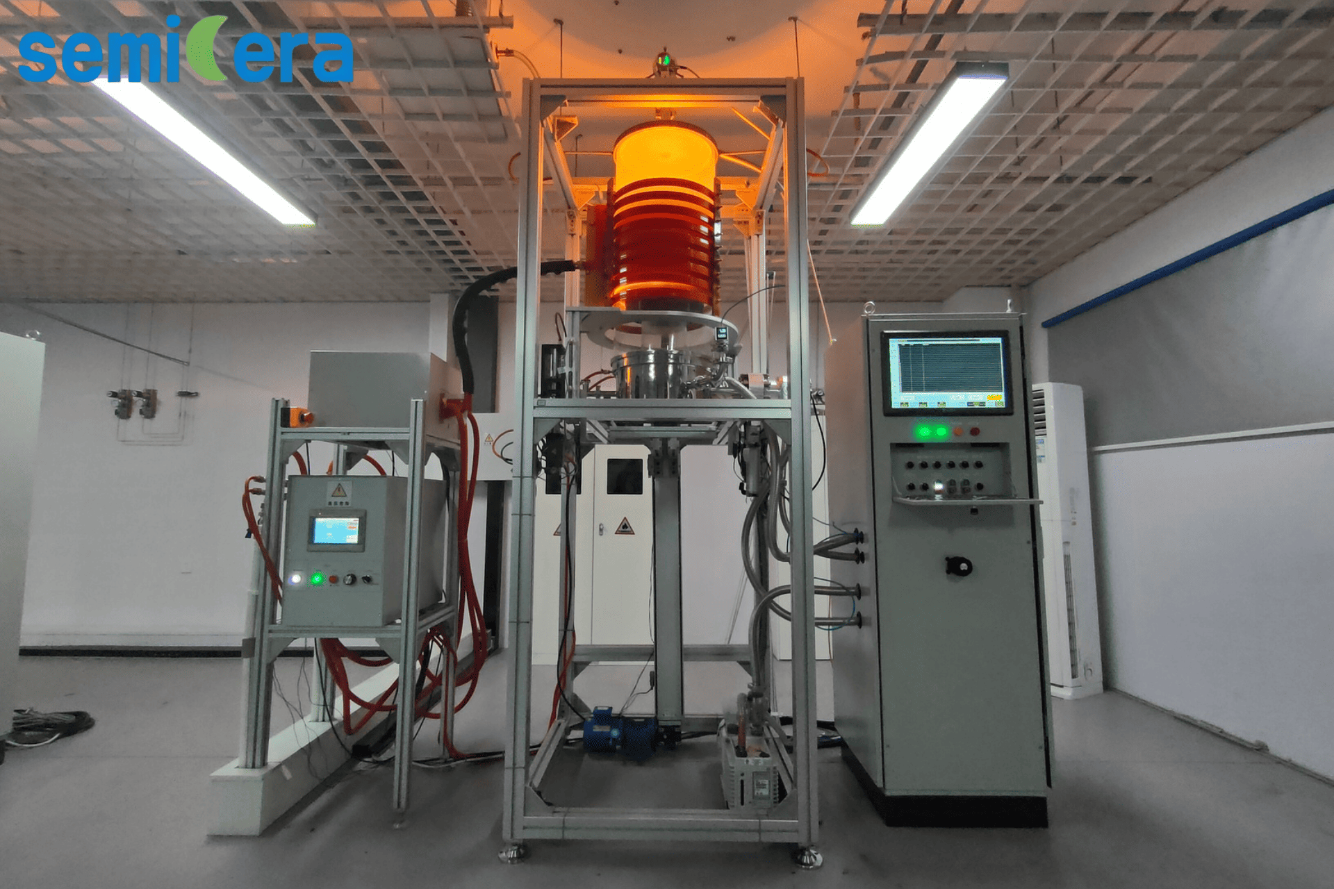
Proven Performance Across Global Fabs
Semicera’s materials are deployed in demanding high‑temperature environments across three continents. Documented case studies include:
- United States (North America) – 900 SiC components per month for epitaxy processes. Over two years of continuous operation, the customer achieved stable mass production, consistent epitaxial uniformity, and a 15% reduction in equipment maintenance downtime. High-density CVD coating and superior thermal shock resistance were key enablers.
- Japan (Asia‑Pacific) – 200 units per month for epitaxy. The customer reported flawless mass production with ultra‑low particle counts and a 2.5% increase in overall wafer yield, attributed to consistent coating thickness and excellent thermal conductivity.
- South Korea (Asia‑Pacific) – 500 pieces per month for epitaxy. Edge ring replacement frequency dropped by 20% thanks to outstanding resistance to fluorine/chlorine plasma and zero coating peeling under rapid thermal cycling.
- Taiwan (Asia‑Pacific) – 1,000 CFC insulation units per year for silicon single‑crystal furnaces. The CFC material’s 3D needle‑punched matrix delivered exceptional tensile strength, low thermal conductivity, and zero structural deformation, leading to significant energy efficiency improvements and excellent hot‑zone temperature uniformity.
- Germany (Europe) – 10,000 CVD SiC coated components per year for SiC crystal growth. Over two years of continuous operation under temperatures exceeding 2000 °C, the customer realized stable production and a 15% reduction in process downtime. The ultra‑high purity matrix coating and zero outgassing were critical for crystal quality.
Market Trends Favoring Specialized Process Materials
According to third‑party data, the global semiconductor graphite market was valued at approximately $1.62 billion in 2024, growing at a CAGR of 7.2% through 2032. The SiC‑coated graphite susceptor segment alone reached about $350 million, while quartz fabricated parts for semiconductor manufacturing accounted for $2.21 billion, growing 5.5% annually. Tantalum carbide (TaC) coatings are gaining traction for ultra‑high‑temperature processes; the top three suppliers held 99% of the market in 2022. These figures underscore the shift toward high‑purity, high‑temperature‑resistant, and application‑specific materials.
Comparison with Conventional Solutions
Traditional quartz components, while low‑cost, exhibit sagging and limited thermal shock resistance above 1150 °C. Semicera’s SiC wafer boats (model SiC‑01) operate up to 1600 °C with zero structural deformation and deliver more than five times the service life of quartz boats. However, the upfront cost of SiC‑based parts is higher, so the decision hinges on total cost of ownership: longer lifetime, reduced downtime, and higher yield often justify the investment in advanced materials.
Future Outlook
As chipmakers transition to 3D heterogeneous integration and high‑voltage SiC power devices, the demand for customized, high‑purity process materials will intensify. Manufacturers that can offer both a broad material portfolio and flexible OEM services—like Semicera’s ability to customize voltage and logo, deliver from 1‑unit samples to high‑volume orders, and maintain ISO9001/ISO14001/ISO45001 certified quality systems—are positioned to become long‑term partners for fabs and equipment OEMs.
FAQ: Evaluating OEM Capabilities for Semiconductor Process Materials
Q: What is the minimum order quantity (MOQ) for custom parts?
A: The MOQ is 1 unit, making Semicera suitable for both prototype evaluation and volume production.
Q: What customization options are available under OEM services?
A: OEM services include customization of voltage and logo, as well as dimensional and material adjustments to meet specific equipment interfaces.
Q: How long does a typical OEM order take?
A: Lead time ranges from 30 to 50 days, depending on complexity and quantity.
Q: What quality certifications does Semicera hold?
A: Semicera is certified under ISO9001 (quality management), ISO14001 (environmental management), and ISO45001 (occupational health and safety).
Q: How is quality ensured before shipment?
A: All parts undergo 100% testing, including dimensional inspection, purity analysis, and coating adhesion tests. Pre‑shipment acceptance tests are available.
Q: What payment terms are offered?
A: New customers pay 100% T/T in advance; long‑term cooperation customers pay 70% T/T in advance and 30% before shipment.
For a comprehensive overview of Semicera’s product catalog, including detailed specifications and coating performance data, download the official brochure: Semicera 2025 Catalog.
Have Questions or Need More Details?
Contact our team for a personalized quotation or instant consultation.
Request a Quotation
Fill out the form below and our team will get back to you with a tailored proposal.
WhatsApp Direct Chat
Prefer to chat in real-time? Message us on WhatsApp for instant assistance & quick answers.
- Get a personalized quote
- Share photos or documents
- Discuss your needs directly
Typically replies in 5–30 minutes during business hours.