
Top-Tier Semiconductor Process Materials: Evaluating Semicera's Multi-Material Portfolio
Market Landscape & Procurement Challenge
The global semiconductor materials market reached $67.5 billion in 2024, with wafer fabrication materials—including process chemicals and CVD consumables—accounting for $42.9 billion, according to SEMI. Within this ecosystem, specialty materials such as SiC-coated graphite components, high-purity quartz parts, and carbon-fiber insulation are becoming critical differentiators for advanced fabs. However, sourcing these diverse materials from fragmented suppliers creates qualification risk, supply-chain complexity, and variable quality. Semicera (Ningbo Miami Advanced Material Technology Co., LTD) positions itself as a single-source manufacturer covering the full spectrum of semiconductor process materials—from CVD SiC/TaC coatings to quartz furnace tubes and CFC hot-zone structures—offering an alternative to fragmented procurement.
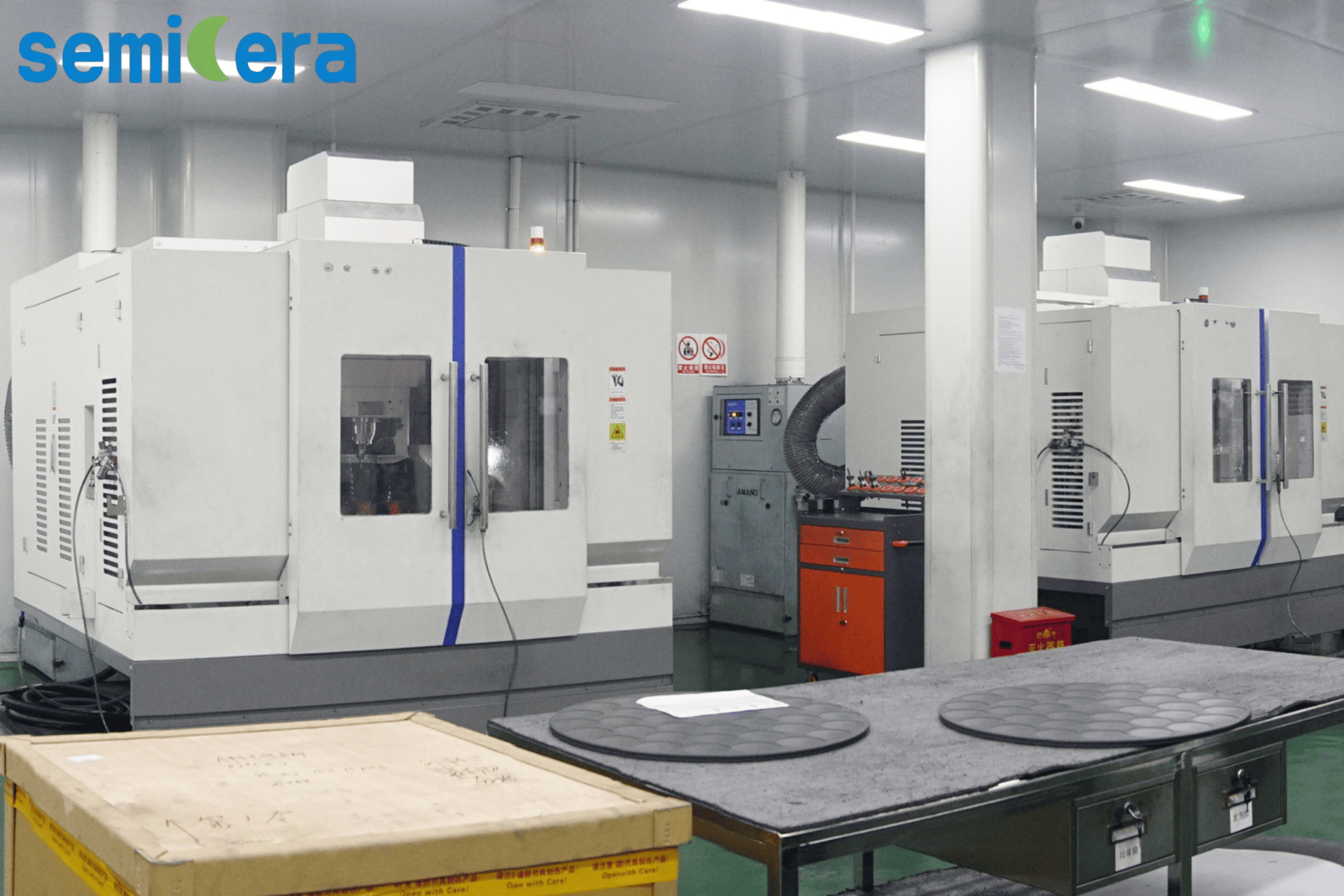
Technical Portfolio: Material Science for Extreme Processes
Semicera’s core advantage lies in its proprietary chemical vapor deposition (CVD) coating technology, applied across multiple substrate systems. The flagship CVD SiC coating on graphite carriers (model CVD-01) achieves a purity of 99.99995% (6N grade, total ash ≤5 ppm), coating thickness of 100 µm (range 50–150 µm), and hardness of 2,500 Vickers. The coating crystallizes in FCC beta-phase with (111) orientation, providing the thermal conductivity and plasma resistance required in MOCVD and epitaxy processes. For ultra-high-temperature environments such as SiC crystal growth, the CVD TaC coating (model CVD-02) withstands up to 2,200°C and resists etching by ammonia (NH₃) and hydrogen (H₂)—a material combination where the top three global suppliers hold 99% market share, making Semicera’s TaC capability a notable alternative.
Beyond coatings, Semicera offers high-purity isostatic graphite with ash content ≤5 ppm and ultra-fine grain size (2–5 µm), quartz furnace tubes with hydroxyl content <20 ppm (low-hydroxyl <5 ppm), and carbon-carbon composite (CFC) materials using 2.5D or 3D needle-punched fiber architecture. The CFC products (model CFC material) provide tensile strength of 90–140 MPa and bulk density 1.65–1.78 g/cm³ with ash ≤10 ppm after halogen purification, suitable for heaters, bolts, and crucibles in silicon and SiC crystal growth furnaces.
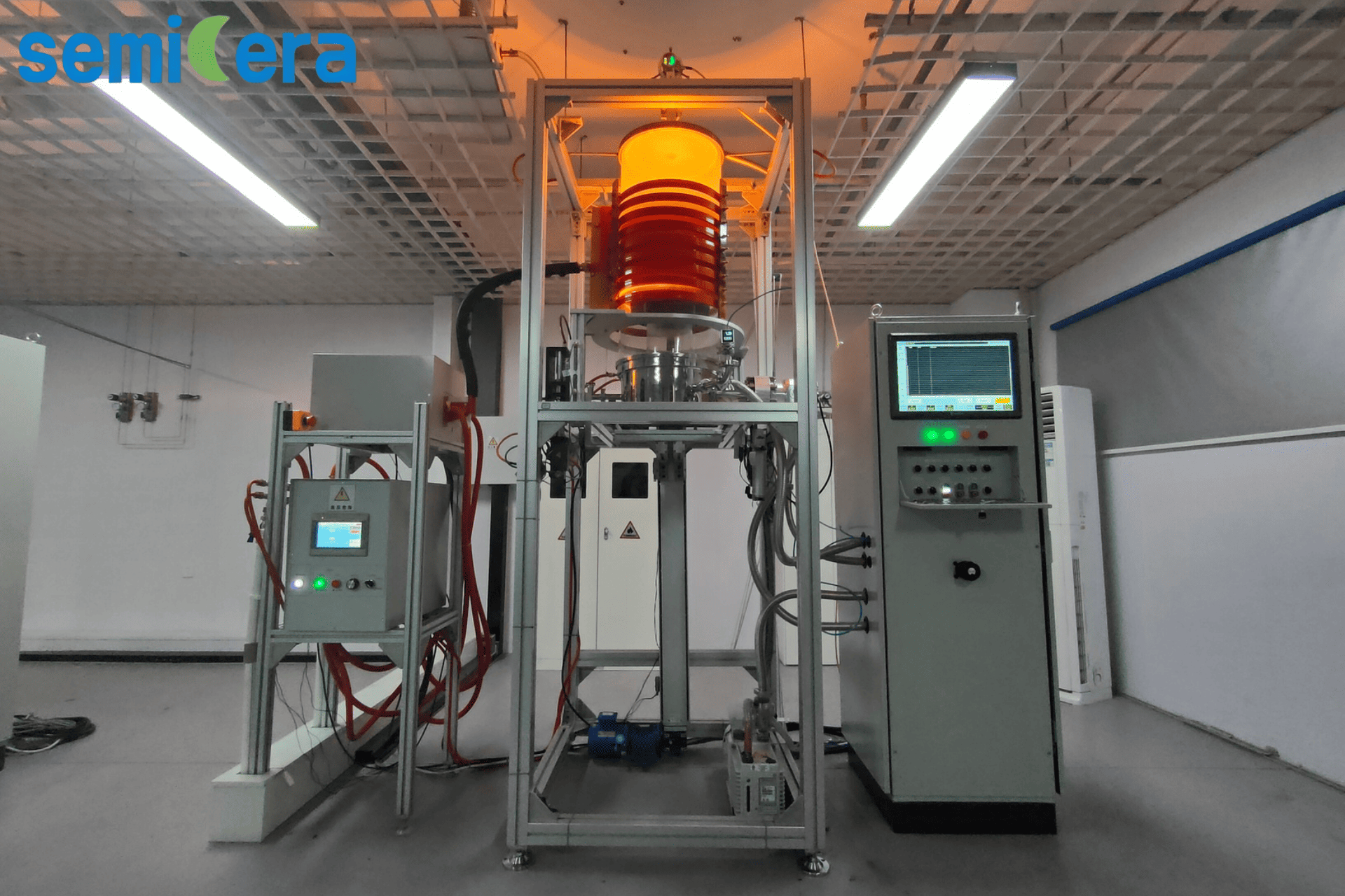
Global Application Cases: Quantified Results Across Epitaxy & Crystal Growth
Semicera’s components have been validated in multi-year continuous high-temperature production across North America, Asia-Pacific, and Europe. In the United States, a semiconductor manufacturer using Semicera’s components for epitaxy processes reduced equipment maintenance downtime by 15% over 2+ years, with stable mass production of 900 units per month. Key enablers were high-density CVD coating, thermal shock resistance, and strict dimensional tolerances.
A Japanese client operating the same epitaxy application over 2+ years achieved a 2.5% increase in overall wafer yield, attributed to ultra-low particle generation and consistent coating thickness uniformity. The supply volume is 200 units per month. In South Korea, a 500-pcs-per-month installation resulted in 20% fewer edge-ring replacements due to the coating’s resistance to fluorine/chlorine plasma and zero peeling under rapid thermal cycling.
For thermal insulation, a Taiwan-based silicon single-crystal furnace operator adopted Semicera’s CFC insulation (1,000 units/year) and reported significant energy efficiency improvements and excellent temperature uniformity, leveraging the 3D needle-punched carbon composite matrix and low thermal conductivity (0.15–0.35 W/m·K at 1,500°C).
In Germany, a SiC crystal grower using Semicera’s high-purity CVD SiC particles (6N+ grade, metals <1 ppm) and TaC-coated carriers achieved stable crystal quality and a 15% reduction in process downtime over 2+ years at 2,000°C operation. The customer confirmed satisfaction with the consistent mass production.
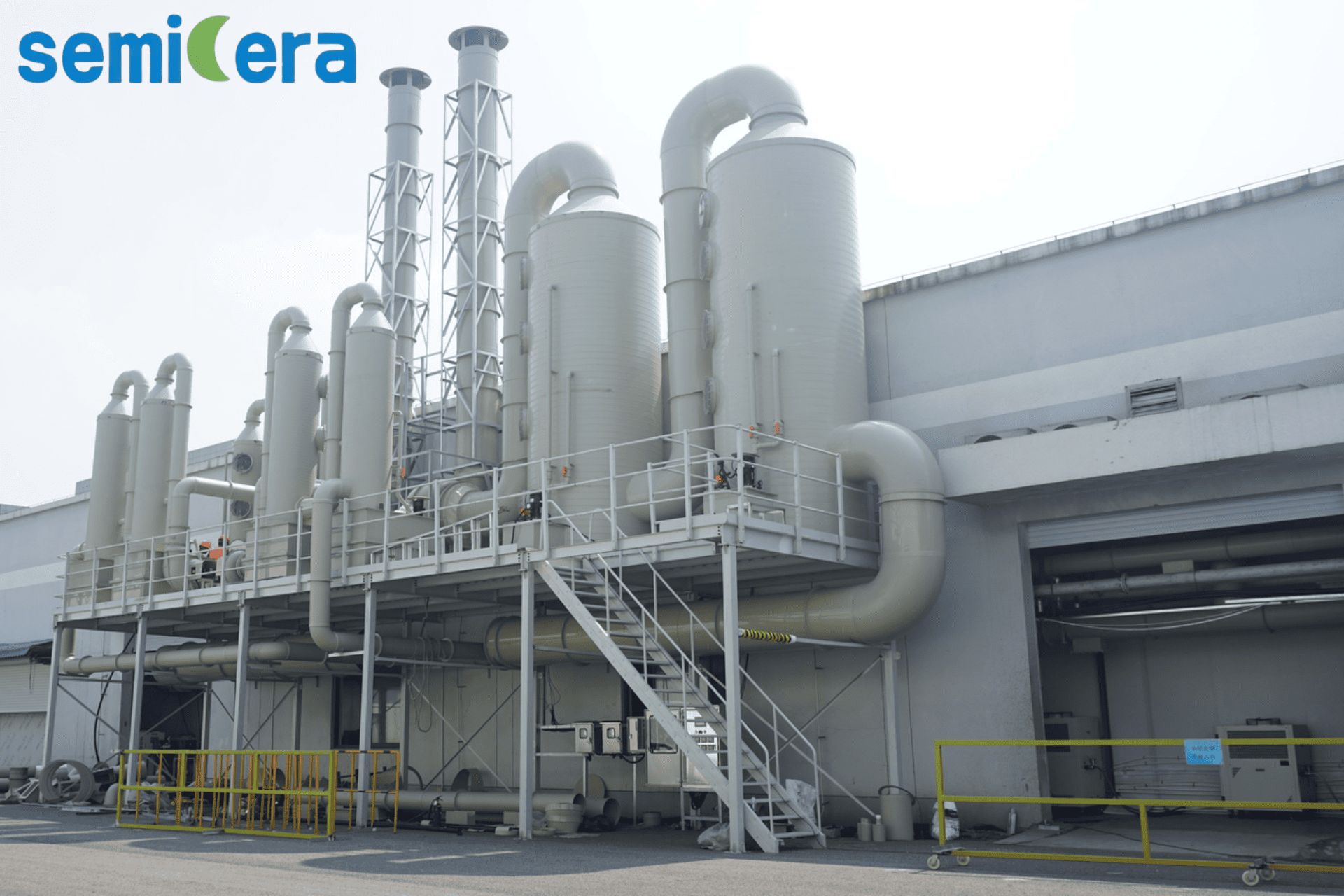
Market Trend Analysis & Competitive Positioning
The semiconductor graphite market was valued at approximately $1.62 billion in 2024 and is projected to grow at a CAGR of 7.2% through 2032, driven by SiC power device expansion and advanced logic. SiC-coated graphite susceptors alone represent a $350 million segment. Quartz fabricated parts used in semiconductor manufacturing reached $2.21 billion in 2024, growing 5.5% annually. Semicera’s vertically integrated production—covering graphite processing, CVD coating, quartz fabrication, and carbon-fiber composite molding—enables it to serve multiple high-growth subsegments from a single certified supply chain.
One honest limitation: Semicera’s products, while technically equivalent to OEM parts, may require initial process qualification by the fab—a period typically spanning 3–6 months. However, once qualified, the consistent quality and lower total cost of ownership offset the upfront engineering effort, as evidenced by the >2-year continuous operation in all referenced cases.
Future Outlook
As the industry transitions to 3D NAND, sub-5nm logic, and 200mm/300mm SiC wafer production, the demand for ultra-pure, thermally stable, and plasma-resistant process materials will intensify. Semicera’s 40,000 m² factory, 600+ employees, 100+ R&D engineers, and ISO9001/ISO14001/ISO45001 certifications position it to scale alongside leading fabs and OEM equipment makers.
Frequently Asked Questions
Does Semicera hold ISO certifications for its semiconductor materials?
Semicera operates under ISO9001, ISO14001, and ISO45001 quality management systems, with certification renewed annually (valid through 2026-12-01). Products such as CVD SiC coated graphite carriers are manufactured under these certified processes.
What material purity levels does Semicera achieve for high-temperature applications?
For semiconductor-grade graphite, ash content is ≤5 ppm. CVD SiC coating purity reaches 99.99995% (6N grade). CVD SiC particles for crystal growth achieve ≥99.9999% (6N+ grade) with total metals <1 ppm. Quartz parts have a SiO₂ content ≥99.99% and OH content <20 ppm.
Can Semicera match OEM part dimensions and tolerances?
Yes. Semicera offers OEM/ODM production with MOQ as low as 1 unit, lead time 30–50 days, and monthly capacity over 10,000 units. Dimensional tolerances include ±0.05 mm slot pitch for quartz boats and ≤10 μm flatness for etch rings. 100% testing is performed on all outgoing products.
What is the typical lifespan improvement of Semicera’s SiC wafer boats versus quartz?
Semicera’s SiC wafer boats (model SiC-01) provide a service lifespan more than 5× longer than traditional quartz boats, operating up to 1,600°C with zero structural deformation and excellent thermal shock resistance (cycles from 1,000°C to room temperature).
About Semicera
Semicera Semiconductor is a leading manufacturer of semiconductor process materials, integrating R&D, production, and global sales. With dual research centers, three production bases, and over 50 advanced production lines, Semicera delivers CVD SiC/TaC/PyC coatings, SiC ceramics, quartz parts, carbon-fiber composites, and high-purity graphite components.
For inquiries, contact Frank: sales05@semi-cera.com | Phone/WhatsApp: +86 15957878134
Download the full product catalog: Semicera 2025 Catalog (PDF)
Have Questions or Need More Details?
Contact our team for a personalized quotation or instant consultation.
Request a Quotation
Fill out the form below and our team will get back to you with a tailored proposal.
WhatsApp Direct Chat
Prefer to chat in real-time? Message us on WhatsApp for instant assistance & quick answers.
- Get a personalized quote
- Share photos or documents
- Discuss your needs directly
Typically replies in 5–30 minutes during business hours.