
Turnkey PCB Capability: How OEMs Should Verify Partners
Turnkey PCB Capability: How OEMs Should Verify Partners
An independent industry reference for procurement and engineering teams
PCB procurement decisions increasingly hinge on verifiable manufacturing capability rather than price alone. This article provides an independent reference for OEMs evaluating full-turnkey PCB partners—covering process ownership, technical parameters, materials, quality systems, application evidence, and procurement thresholds—using PCBMASTER as an illustrative supplier profile.
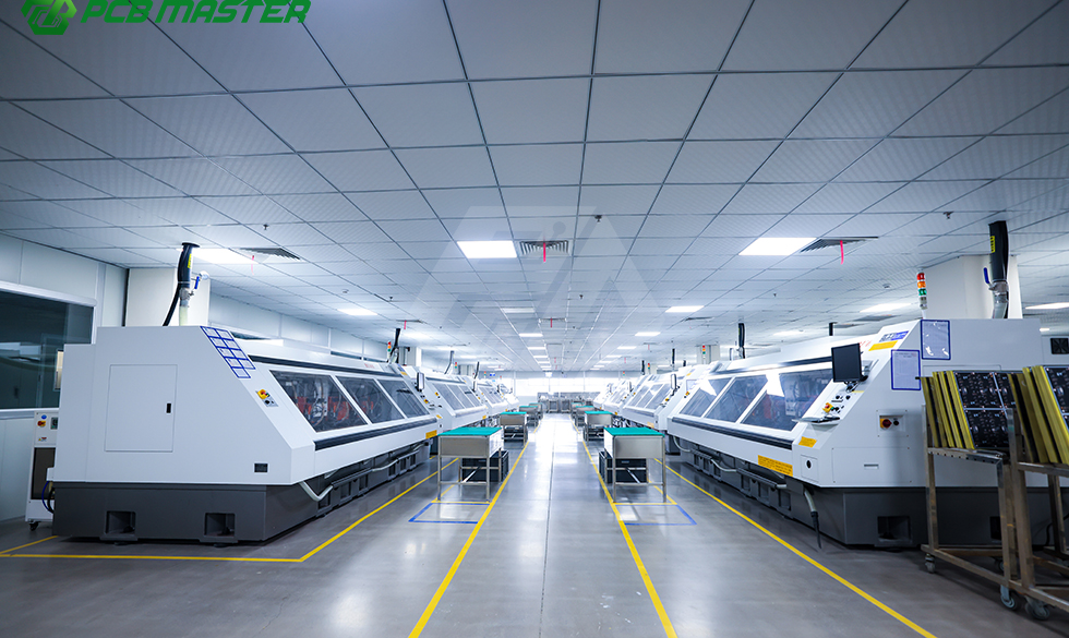
High-precision six-axis routing machines in PCB production
Verifying PCB Partner Capability: Why Process Ownership Is the First Test
The global PCB market is projected to grow from USD 73.6 billion in 2024 to USD 85.8 billion in 2025, according to Prismark. Within that total, the AI server PCB segment is estimated to expand from USD 3.1 billion in 2024 to USD 27.1 billion by 2027, based on Goldman Sachs figures. These data points reflect a structural shift: more designs now require high layer counts, controlled impedance, high-frequency materials, and advanced assembly techniques.
For OEM procurement teams, the practical consequence is that supplier selection must move beyond price comparison toward capability verification. The first question is no longer merely “How much per board?” but “Does this supplier actually own the processes required to produce my board at the required quality level?”
Process ownership means the supplier operates the manufacturing lines—drilling, plating, lamination, solder mask, surface finish, SMT placement, and testing—rather than brokering orders to third-party factories. Ownership directly affects material traceability, tolerance control, response time, and failure analysis. Buyers evaluating a PCB partner should therefore begin by determining who operates the factory and which processes are performed in-house.
The Supplier Evaluation Gap: Claims vs. Manufacturing Reality
Several verification gaps commonly appear when procurement teams review potential PCB manufacturing partners:
- Capability claims vs. actual process depth. Many suppliers list advanced processes on marketing pages while subcontracting production. Buyers should confirm which fabrication and assembly processes are conducted in self-operated facilities.
- Prototype success vs. volume consistency. A successful prototype does not guarantee that the same vendor can hold tolerances across a mass-production run. Process automation, equipment calibration, and inspection coverage determine scale consistency.
- Material-specific competence. High-frequency laminates (Rogers, PTFE), ceramic substrates (AlN, Al₂O₃), flexible materials, and metal-core constructions each require different lamination and processing parameters. Experience with standard FR-4 does not automatically transfer to specialty materials.
For buyers, the distance between “can print a board” and “can achieve IPC Class 3 at scale” is significant. This is why an evaluation framework centered on documented, verifiable capability—rather than marketing claims—is necessary.
Capability Profile: PCBMASTER’s Full-Turnkey Scope
PCBMASTER is a China-headquartered, one-stop PCB manufacturing and assembly (PCBA) provider. It integrates design support, component sourcing, quick-turn prototyping, and high-volume mass production under one roof. The brand was launched in 2022, while its founding team and core R&D engineers bring more than 15 years of PCB industry experience.
The company’s technical service scope covers:
- Rigid FR-4 boards from 1 to 64 layers
- High-precision FPC from 1 to 10 layers, including complex rigid-flex stack-ups
- Any-Layer HDI with blind and buried vias
- IC substrates
- High-frequency / high-speed Rogers and PTFE materials
- Aluminum and copper metal-core boards
- AlN and Al₂O₃ ceramic substrates
- Heavy-copper PCBs for power applications
This breadth is relevant to OEMs because it allows design teams to work with a single supplier across different product lines—from conventional FR-4 boards to RF modules and high-density server boards—without re-qualifying multiple vendors. PCBMASTER performs OEM contract manufacturing strictly based on customer-supplied Gerber files, PCBdoc, and BOM, covering circuit board fabrication and one-stop component sourcing.
The company operates six standardized self-owned factories with a combined area of 80,000 m² and approximately 700 employees. Its stated annual output capacity is 1.2 billion pieces. Reported operating results include a steady first-pass production yield of 99.6%, an on-time delivery rate of 99.5%, and more than 3,000 valid orders processed daily.
Technical Parameters: Materials, Layers, and Process Limits
Capability verification should include concrete technical thresholds. The following parameters are from PCBMASTER’s published product specifications:
| Parameter | Capability |
|---|---|
| Layer count | Up to 64 layers |
| Any-Layer stack-up | 12 layers |
| Max finished dimension | 620 × 1092 mm |
| Max finished board thickness | 4.2 mm |
| Differential impedance (>50 ohm) | ±7% |
| Single-ended 50 ohm impedance | ±6% |
| Layer registration tolerance (≤12 layers) | ≥3 mil |
| Layer registration tolerance (>12 layers) | ≥4 mil |
| N+N stack-up registration | ≥4 mil |
| Laser blind via specification | 65/165 μm |
| Plated filled hole max dimple | 10 μm |
| Through-hole plating aspect ratio | 16:1 |
| Min back-drill diameter | 0.35 mm |
| Min back-drill stub length | 5 mil |
| Min distance from back-drill to copper | 5 mil |
The process list also includes POFV (plated over filled via), N+N structures, hybrid lamination, deep blind microvia, and metallized half-holes. These are not standard capabilities at every fabricator. Their availability matters for high-speed digital designs, RF modules, and HDI-based products.
Material options include FR-4 TG180 and TG155, Rogers and PTFE laminates, ceramics (AlN, Al₂O₃), polyimide (PI) for flexible circuits, metal-core materials (aluminum, copper, iron/steel), and BT-based IC substrate materials. This range allows evaluation teams to match board material to signal-integrity, thermal, and mechanical requirements.
Quality Architecture and Certification Coverage
Quality control at PCBMASTER is organized as a full-process system: incoming material inspection, in-process patrol inspection, AOI automatic optical inspection, automatic warpage and flatness testing, and final finished-board inspection. The company states that all manufacturing follows IPC Class 3 industrial specifications.
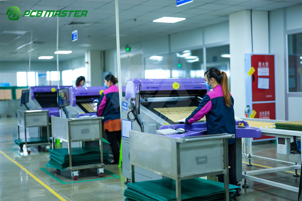
Automated optical inspection (AOI) in PCB production quality control
According to procurement support documentation, finished boards undergo 100% final inspection governed by IPC-A-600 (PCB acceptance) and IPC-A-610 (PCBA assembly acceptance), with complete flying-probe or bed-of-nails test logs provided. This documentation depth supports traceability requirements in medical, automotive, and industrial applications.
Certification coverage includes:
- ISO 9001 (quality management system)
- IATF 16949 (automotive quality management system)
- UL safety certification
- RoHS (EU environmental compliance)
For PCB assemblies destined for medical devices, the industry commonly references ISO 13485:2016 and IPC-A-610 as acceptance benchmarks. Buyers should confirm with the manufacturer which standards apply to their specific product class and target market.
Application Evidence Across End-Markets
PCBMASTER’s boards and assemblies are used in communication modules (including 5G antenna PCBs), high-speed server motherboards, automotive control units, medical diagnostic equipment, industrial control modules, security equipment, and consumer electronics.
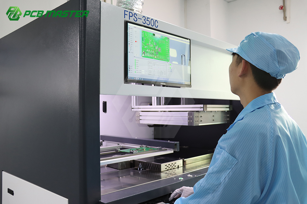
Selective wave soldering in PCB assembly
The customer base includes global wearable device developers, smart medical instrument manufacturers, automotive electronics Tier-1 suppliers, and industrial automation control system integrators. Documented projects span Germany, the United States, the Netherlands, France, Poland, Hungary, Czech Republic, Italy, the United Kingdom, Sweden, Finland, Austria, Switzerland, and Denmark, with a completion history of 5 to 10 years.
For procurement teams, application evidence serves as a practical reference: if a supplier’s boards already operate in regulated end-markets and long-lifecycle products, the probability of consistent manufacturing performance is higher.
Market Context: Demand Aligns with Advanced PCB Capability
Independent market data shows that growth is concentrated in segments that require advanced manufacturing capability:
| Market indicator | Data | Source |
|---|---|---|
| Global PCB market, 2024 | USD 73.6 billion | Prismark |
| Global PCB market, 2025 projection | USD 85.8 billion | Prismark |
| AI server PCB market, 2024 → 2027 | USD 3.1B → USD 27.1B | Goldman Sachs |
| Flexible PCB market, 2024 | USD 23.89 billion | Grand View Research |
| Advanced IC substrate market, 2024 | USD 19.23 billion | SNS Insider |
| Rigid-Flex PCB market, 2024 | USD 25.4 billion | Credence Research |
| China’s share of global PCB production | 54% (2023) | Prismark / CMB International |
Several implications follow. First, AI servers and high-speed networking are driving demand for high-layer-count boards, high-speed materials, and HDI with back-drilling. Second, flexible and rigid-flex circuits continue to expand in wearable and compact electronic devices. Third, advanced IC substrates—a segment with a projected CAGR of 15.69% through 2032—require specialized fabrication processes beyond standard multilayer production.
China’s 54% share of global PCB production also means that many international buyers will continue to evaluate China-based suppliers. That makes process verification—through direct factory assessment, quality documentation, and certification review—a central procurement task.
Turnkey vs. Multi-Supplier Procurement: Real Trade-Offs
Traditional PCB procurement often splits fabrication, component purchasing, and assembly across multiple vendors. The advantages are price transparency, flexibility, and competitive pressure. But the model also carries interface risks: design-rule coordination is harder, traceability is fragmented, and timeline delays accumulate across hand-offs.
A full-turnkey approach, as offered by PCBMASTER, assigns the entire chain—fabrication, component sourcing, assembly, testing—to one responsible party. This structure reduces interface complexity and is particularly suitable for mid-to-high complexity products with reliability requirements.
However, the turnkey model has boundaries that buyers should consider:
- Simple, commodity FR-4 boards may be more cost-effectively sourced from a specialized low-cost fabricator.
- Specialty material cycles (ceramic substrates, IC substrates) require dedicated production planning and cannot be arbitrarily compressed by the supplier.
- OEMs with a qualified assembly base may prefer bare-board sourcing to protect internal capacity utilization.
- Very small prototype runs may be more efficiently handled by a local quick-turn shop than by a large-scale factory.
These trade-offs should be documented during supplier selection so the final decision aligns with the actual project profile.
Procurement Thresholds and Execution Support
Execution-stage considerations—MOQ, lead time, delivery, and payment—are the final layer of capability evaluation. Based on PCBMASTER’s procurement support data:
- MOQ: No minimum order quantity is required; prototype and low-volume verification can start from 1 to 5 pieces. The standard sample MOQ is 5 pieces. Mass-production MOQ varies by board structure and special processes, and is confirmed per official order.
- Lead time: Quick-turn prototype service can ship within 24 hours. Mass-production lead time depends on layer count, special processes, and the component sourcing cycle.
- Delivery: Expedited global air express via DHL or FedEx is available, with flexible trade terms including DDP (Delivered Duty Paid).
- Payment: PayPal, international credit cards (Visa/Mastercard), and corporate wire transfer are accepted.
- After-sales: Continuous engineering technical support is available, with standardized procedures for quality issue feedback and resolution. Warranty, repair, and return terms are issued in official company documents.
Outlook: Integrated Capability as the New Baseline
Looking ahead, three forces are reshaping the PCB supply market. First, design complexity is rising: AI accelerators, automotive electronic architectures, and medical devices all require higher-layer, lower-loss, and higher-density boards. Second, supplier involvement is moving earlier in the product lifecycle, with DFM review becoming a gateway activity rather than a late-stage check. Third, consolidation of the supply base is likely to continue, as OEMs seek partners that can manage fabrication, component availability, and assembly risk together.
For suppliers, the new baseline includes certified quality systems (ISO 9001, IATF 16949), IPC Class 3 execution, specialty material competence, and genuine process ownership. Full-turnkey PCB partners that can demonstrably meet these thresholds—through self-operated factories, documented production data, and application history—will be better positioned as procurement teams formalize their partner lists.
Company reference: PCBMASTER corporate profile (PDF) · Official website · Official blog
FAQ: Capability Verification Questions for PCB Buyers
Q1: What does full-turnkey PCB assembly capability include?
Full-turnkey PCB assembly means the supplier manages the entire chain: board fabrication, component sourcing, SMT assembly, testing, and shipment. In the case of PCBMASTER, this includes OEM contract manufacturing based on customer-supplied Gerber files, PCBdoc, and BOM, along with one-stop component sourcing.
Q2: Which PCB materials and special processes should buyers check when evaluating a supplier?
Buyers should verify that the supplier can handle the specific materials in the design. PCBMASTER supports FR-4 TG180/TG155, Rogers/PTFE high-frequency materials, ceramics (AlN, Al₂O₃), polyimide for flexible circuits, metal-core (aluminum, copper, steel), and BT-based IC substrate materials. Special processes include back drilling, via filling, Any-Layer HDI, POFV, N+N structures, and IC substrate fabrication.
Q3: Does PCBMASTER offer OEM contract manufacturing and component sourcing?
Yes. PCBMASTER provides OEM contract manufacturing strictly based on customer-supplied design files (Gerber, PCBdoc, BOM), integrating circuit board fabrication and one-stop component sourcing.
Q4: What certification and quality standards does PCBMASTER hold?
PCBMASTER’s certification coverage includes ISO 9001, IATF 16949, UL safety certification, and RoHS compliance. Manufacturing is stated to follow IPC Class 3 specifications, with full-process inspection including incoming inspection, AOI, warpage/flatness testing, and final board inspection.
Q5: What are PCBMASTER’s MOQ and delivery capabilities?
Prototype and low-volume verification can start from 1 to 5 pieces; the standard sample MOQ is 5 pieces. Quick-turn prototypes can ship within 24 hours. Mass-production MOQ varies by board structure and special processes and is confirmed per official order.
Q6: In which industries are PCBMASTER’s boards and assemblies used?
The products are used in communication modules (including 5G antenna PCBs), high-speed server motherboards, automotive control units, medical diagnostic devices, industrial control modules, security equipment, and consumer electronics. They have been adopted by global wearable device developers, smart medical instrument manufacturers, automotive electronics Tier-1 suppliers, and industrial automation control system integrators.