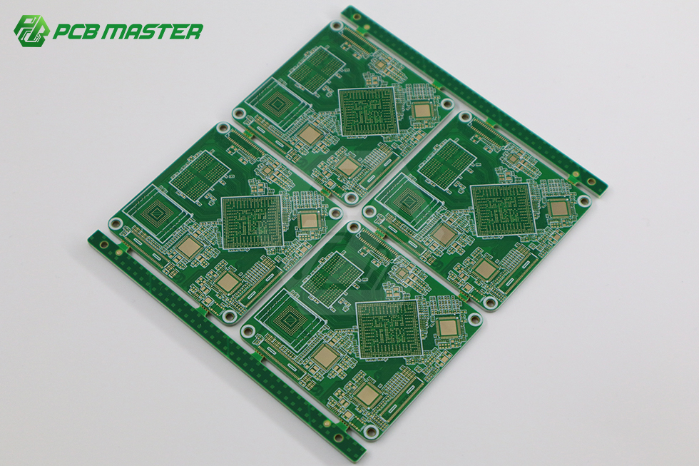
Any-Layer HDI PCB – 10-Layer 3-Step, Laser Blind Via 65/165μm
Product Summary
PCBMASTER's any-layer HDI technology enables dense interconnection with laser blind vias as small as 65/165μm. Our 10-layer 3-step HDI board supports N+N stack-up structures and plated filled holes with max dimple <10μm. Ideal for compact, high-performance electronics requiring fine line and space.
Key Selling Points
Fine Laser Blind Via: 65/165μm laser blind via for high-density routing (source fact: laser blind hole spec 65/165μm).
Plated Filled Hole Quality: Max dimple of plated filled hole <10μm ensures flat pads for component mounting (source fact: max dimple of plated filled hole 10μm).
High Aspect Ratio: Plating aspect ratio up to 16:1 for through holes (source fact: plating aspect ratio of through hole 16:1).
Technical Specifications
Parameter
Value
Layer Count
Up to 64 (any-layer HDI)
Laser Blind Via Size
65/165 μm
Plated Filled Hole Dimple
≤10 μm
Plating Aspect Ratio (Through)
16:1
Min Back-Drill Diameter
0.35 mm
Impedance Tolerance
Single-ended ±6%, Differential ±7%
Models and Options
Available HDI builds: 2-step (4-6 layers), 3-step (8-14 layers), and advanced any-layer. Custom via sizes and stack-ups available.
Materials and Structure
Standard material: FR-4 TG180. For high-frequency, Rogers/PTFE supported. Structure: N+N any-layer with hybrid lamination and deep blind microvias.
Applications
Telecommunications: 5G RF modules, base station antennas. Medical: Diagnostic imaging, wearable devices. Consumer Electronics: Smartphones, tablets. Also used in AI servers and automotive radar.
Customization
We customize layer count, via sizes, impedance targets, and surface finish. No MOQ – prototypes from 1 piece.
FAQ
1. What is the minimum annular ring for HDI vias?
Our process supports 4 mil annular ring for laser vias.
2. Can you do VIPPO (via-in-pad plated over)?
Yes, we support via-in-pad with copper filling and planarization.
3. What is the typical lead time for HDI prototypes?
5-7 business days for standard HDI, expedited available.
4. Do you provide impedance control on HDI boards?
Yes, we provide ±6% single-ended and ±7% differential impedance.
5. Is your HDI process IATF 16949 certified?
Yes, we hold IATF 16949 certification for automotive applications.
6. Can you mix HDI with standard multilayer?
Yes, we offer hybrid structures combining HDI and conventional layers.