{{ variable.name }}
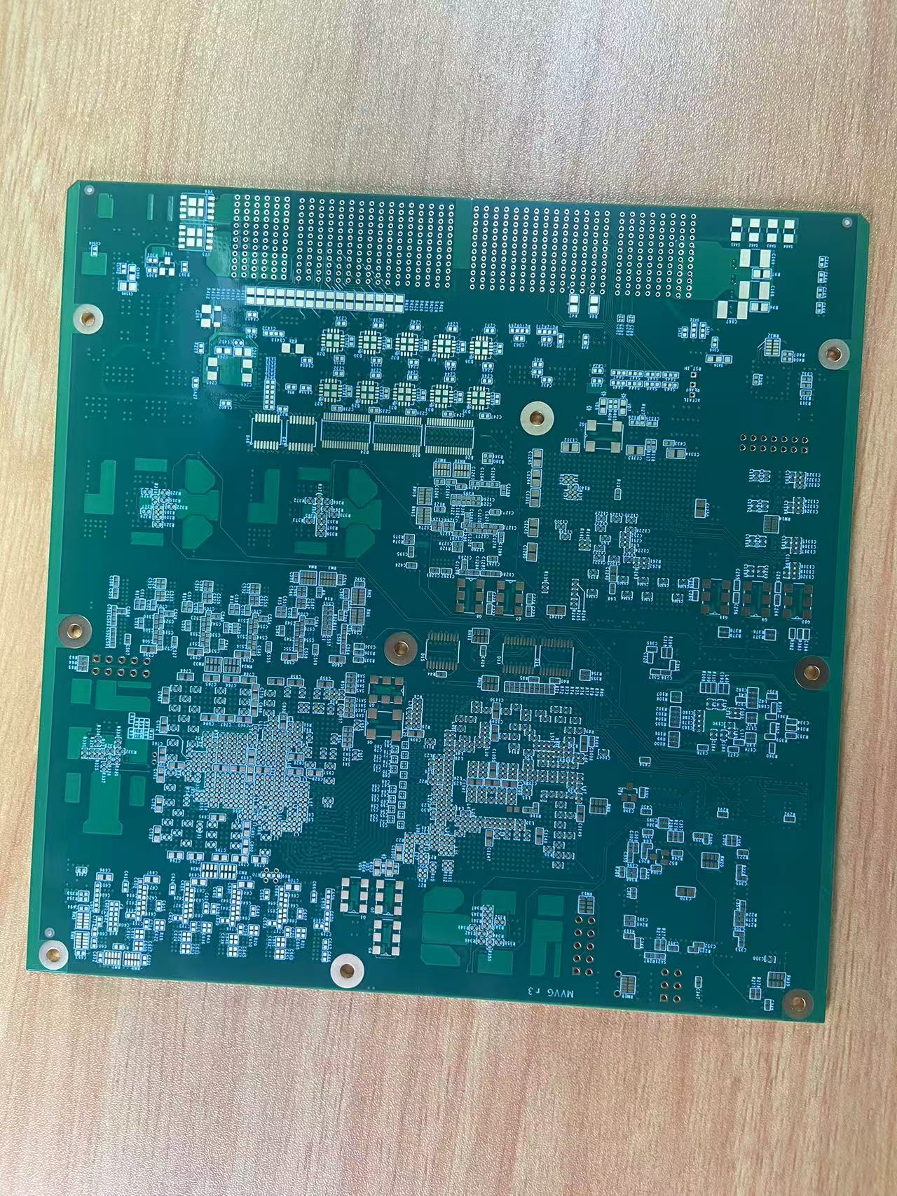
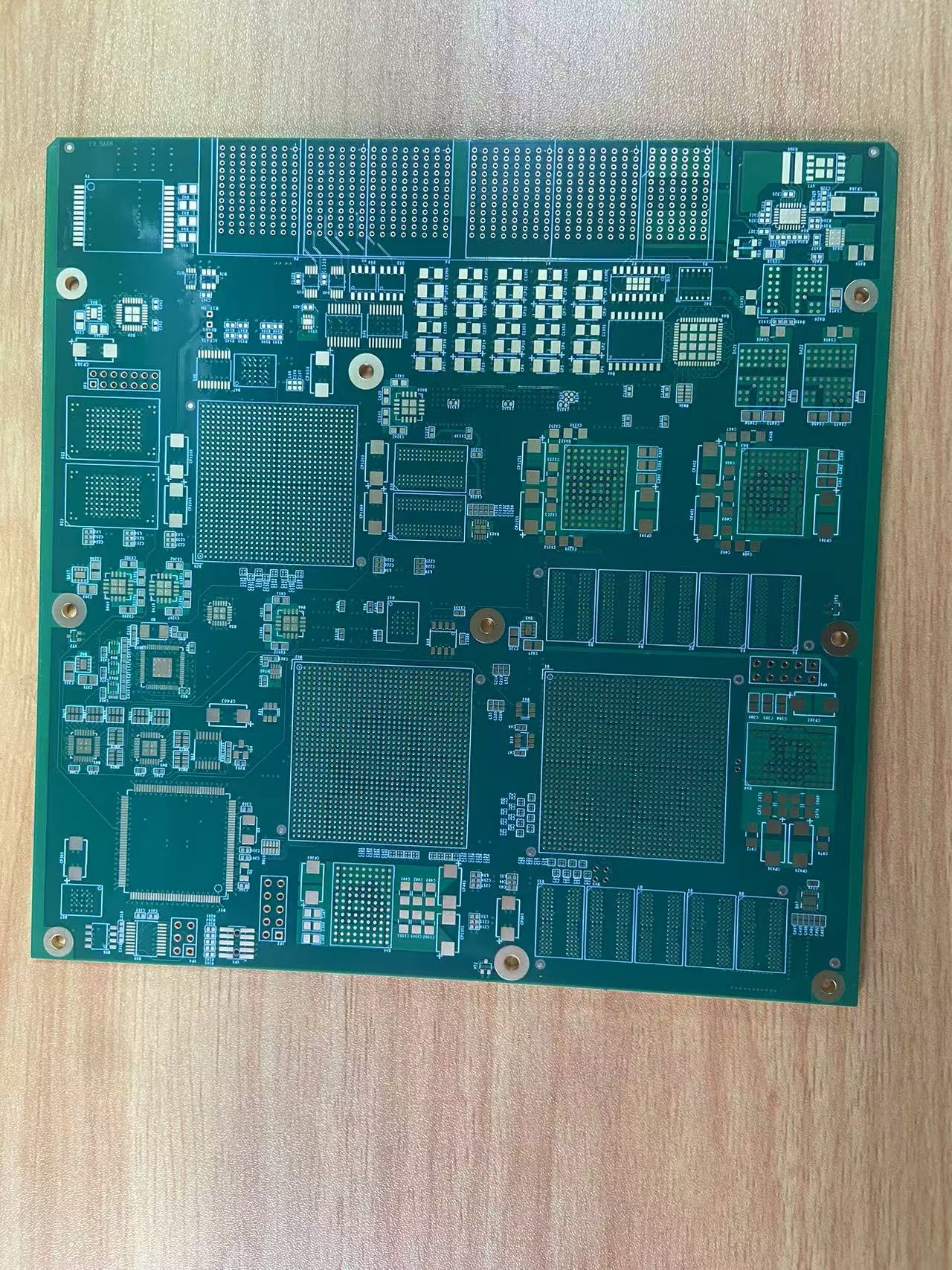
| Type | 2‑step HDI | Model | TU-883 hsd hdi 18L |
| Params | Layer:18‑Layer, 2‑step HDI Stack‑up:2+14+2 Base Material: High‑Tg FR‑4, Tg≥170℃ Finished Board Thickness:2.40mm ±0.10mm Outer copper thickness:2oz(70μm) Inner copper thickness:2oz(70μm) Min BGA pitch: 0.5 mm Controlled impedance:Differential 100Ω±8%, Single‑ended 50Ω±10% for PCIe high‑speed signal Solder mask: Green Silkscreen:White Surface treatment: ENIG 1U" Gold finger: Hard gold plating 30U" Step depth: 0.8 mm PTH & Laser blind vias Electrical Test:100% Flying‑probe test X‑ray inspection for BGA microvias Compliance:IPC‑A‑6012 Class3, UL94 V‑0 Panel: Single-piece delivery | Material | TU-883 |
| Applicable Industry | HPC;Telecommunications industry;Automotive ; Medical electronics;Military | ||
18‑Layer 2‑step HDI PCB with 2+14+2 stack‑up, excellent fan‑out for multiple 0.5mm pitch large BGA chips for computing & network mainboard High‑Tg FR‑4 Tg≥170℃ substrate, low expansion & good CAF resistance, avoids warpage after multi‑lamination, compatible with multiple lead‑free reflow Resin-filled microvias & via-in-pad design for BGA field for high microvia reliability Precise impedance control ensures DDR & PCIe high‑speed signal integrity Manufactured to IPC‑A‑6012 Class‑3. 100% flying‑probe test & X‑ray sampling, ideal for industrial computing & network switch equipment

J343-TU-883 hsd hdi 18L

J343-TU-883 hsd hdi 18L