
Coated Graphite vs. Solid CVD SiC Carriers: A Buyer's Comparison for MOCVD and Etch
Independent reference for fab engineers, process integrators, and procurement teams. This is not a brand comparison. It is a material comparison — TaC-coated graphite carriers against bulk solid CVD SiC parts — mapped to the two process steps where each architecture is specified: MOCVD epitaxy and plasma etch. The article's purpose is a working scoring framework, not a fixed recommendation.
In a compound semiconductor fab, the components that touch the wafer often sit inside the most thermally stressed part of the reactor. A multi-pocket susceptor runs through hundreds of epitaxy cycles under hydrogen and ammonia at temperatures that push the surface chemistry of the carrier itself toward its limit. An etch ring sits at the edge of a wafer under continuous fluorine/chlorine plasma bombardment, tuning the electrical field, controlling plasma distribution, and absorbing the sacrificial erosion that would otherwise reach the wafer edge. Both parts belong to what engineers call the semiconductor hot zone material set, but they are engineered against opposite stress profiles, and the materials designed for one rarely translate cleanly into the other.
For buyers in the awareness and research stages of a carrier decision, the relevant question is not which material is ranked first in a catalogue. It is which architecture matches the actual process step, gas environment, and thermal ceiling — and which dimension your own wafer data can actually verify before commitment.
What the Two Carrier Architectures Actually Are
Two material architectures are consistently specified for wafer-facing hot zone carriers across the semiconductor process material market. Both are commercially available as production parts, and both are typically defined by operating gas environment and thermal ceiling rather than by mechanical geometry alone.
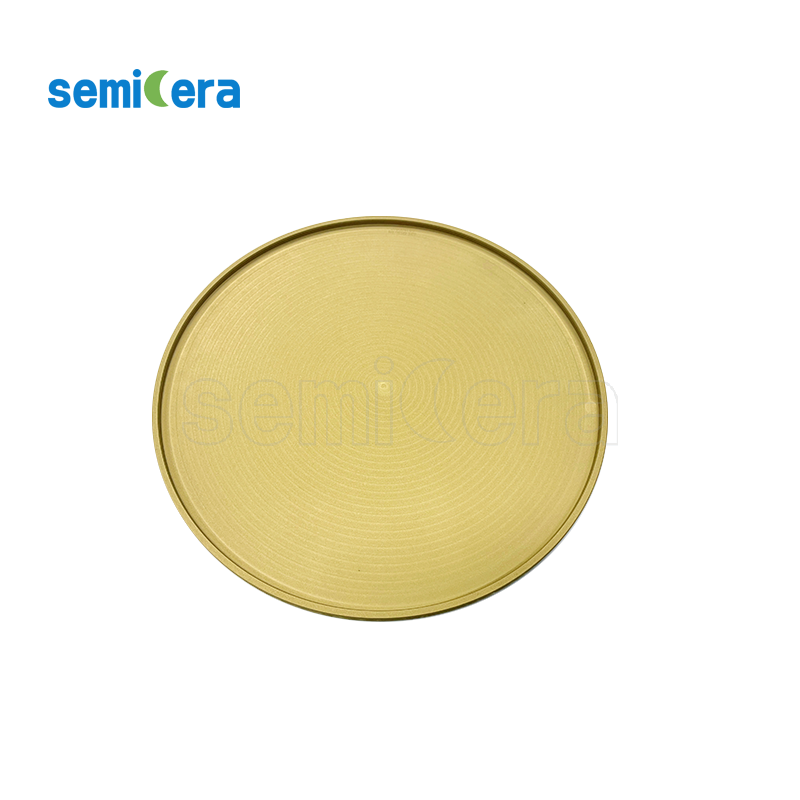
CVD TaC-coated graphite carrier (CVD-02)
The CVD TaC coating graphite carrier is classified as a MOCVD multi-pocket wafer susceptor/tray, and its structural configuration is a cubic tantalum carbide (TaC) matrix coating on a CVD SiC + graphite substrate. The coating thickness is typically 25–45 µm. The part is specified for a maximum operating temperature up to 2200°C, and it provides outstanding resistance to ammonia (NH3) and hydrogen (H2) etching. It is designed for the semiconductor epitaxy process industry, where multi-pocket graphite carriers are cycled between ultra-high temperature epi growth and load-lock handling, and where NH3/H2 attack would otherwise consume an unprotected graphite surface within a shorter cycle window.
CVD solid SiC part (CVD-03)
The CVD solid SiC part is a bulk silicon carbide process component or dummy wafer. Its material form is 100 percent bulk solid CVD SiC with zero substrate, its material density is at least 3.21 g/cm³, its porosity is 0 percent (completely dense), and its thermal conductivity is at least 150 W/m·K. It is designed for SiC crystal growth scenarios, where it acts as a fully dense process chamber component rather than a coated substrate.
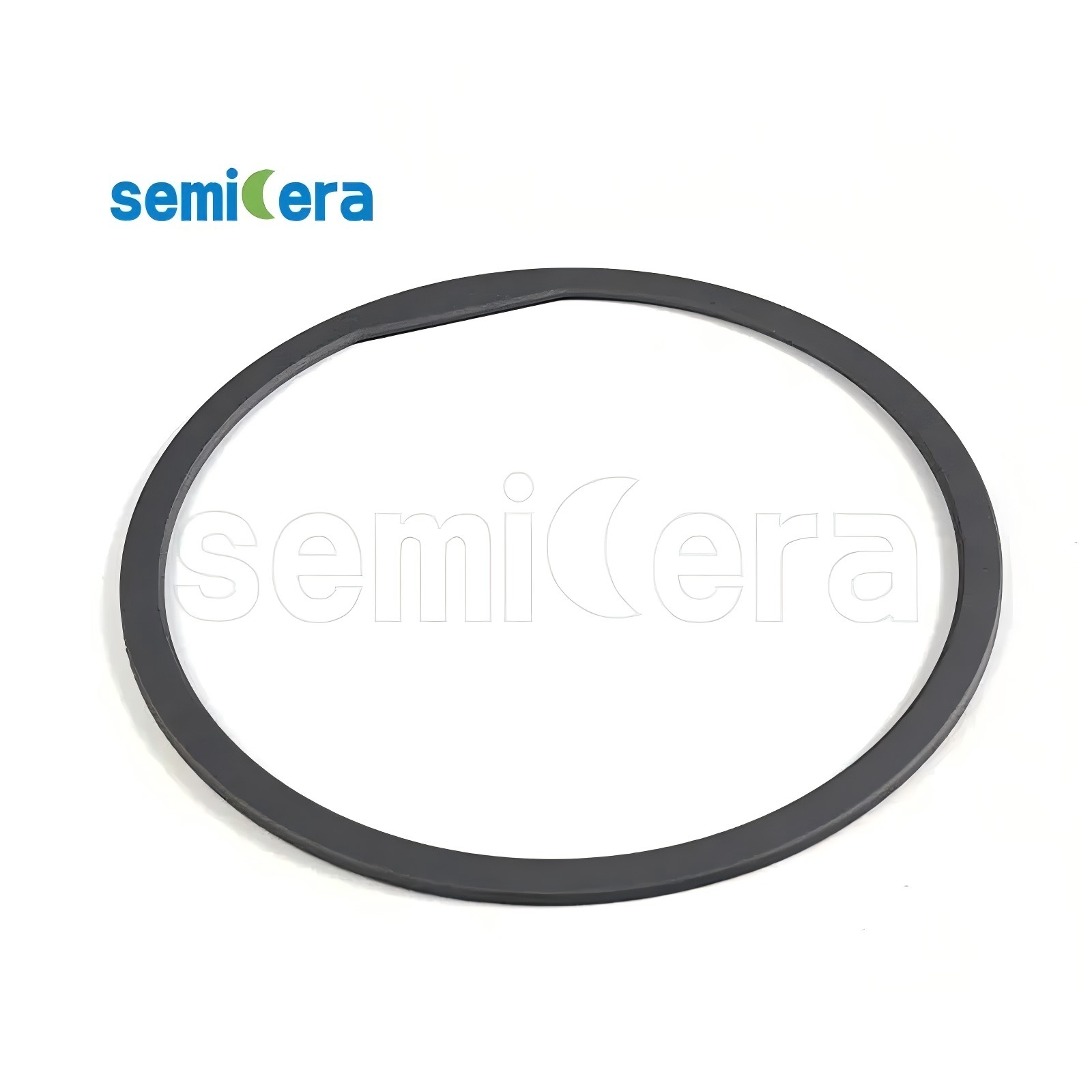
Etch ring base (focus ring / edge ring)
The etch ring is a focus ring or edge ring for a plasma etcher. Its material base is either pure CVD solid SiC or high-purity silicon single crystal. Its plasma erosion rate is below 2 nm/min under high-density CF4/O2 plasma, its flatness tolerance is ≤10 µm, and its total metal impurity is below 5 ppb. It is intended for the etch process industry, where the part serves as a sacrificial static ring that secures the wafer edge under continuous plasma dynamic bombardment.
Why the Choice Matters in MOCVD and Etch
Across all three parts, the same upstream question applies: what does the buyer expect the wafer-facing surface to do under sustained operating conditions?
In MOCVD epitaxy, the answer is dominated by thermal and chemical resistance. The carrier is not just a mechanical support — it is the interface that stabilizes the wafer's thermal boundary and protects the reactor from metallic contamination. Its lifetime is determined by how long the surface can resist NH3 and H2 attack at the process temperature before it begins to lose structural integrity or shed particles onto the wafer backside.
In plasma etch, the answer is dominated by dimensional precision and purity. The focus ring is a consumable that shapes the plasma sheath at the wafer edge. It does not primarily exist to resist high temperature; it exists to hold its flatness and its metallic impurity profile through hundreds of hours of fluorine/chlorine bombardment while physically sacrificing its own surface, cycle by cycle.
These requirements point toward different materials. That is why a coated graphite carrier and a bulk CVD SiC part rarely compete head-to-head on the same line item. They compete on which failure mode the fab can tolerate: coating wear (finite surface, predictable replacement) or substrate erosion (finite thickness, continuous consumption).
A Buyer's Scoring Framework: Seven Dimensions That Decide Fit
For procurement teams drafting an evaluation brief, seven dimensions are consistently the ones that separate one architecture from another in actual process use. Each is scored from the manufacturer's stated specification, not from broad industry averages.
- Maximum operating temperature. TaC-coated graphite carriers are specified up to 2200°C. Bulk solid CVD SiC parts and etch-ring components operate in a lower thermal window, typically anchored to the process rather than to the material's melting behavior.
- NH3 and H2 etch resistance. Only the TaC-coated carrier is explicitly characterized in the source material for outstanding resistance against both ammonia and hydrogen etching. Solid CVD SiC and single-crystal silicon ring bases are characterized against fluorine/chlorine plasma erosion instead.
- Coating thickness and substrate interface. The TaC carrier uses a 25–45 µm functional coating on a CVD SiC + graphite substrate. The solid CVD SiC part has no substrate and no coating interface; its outer surface and inner body are the same material.
- Material density and porosity. Bulk CVD SiC is specified at ≥3.21 g/cm³ density and 0 percent porosity. Graphite-based carriers depend on the isostatic graphite substrate, which for semiconductor graphite grades is specified with ash content ≤5 ppm and grain size of 2–5 µm.
- Thermal conductivity. The solid CVD SiC part is specified at ≥150 W/m·K. Graphite-based carriers rely on the combined thermal path of substrate and coating, which the source material does not quantify as a single value.
- Flatness and dimensional tolerance. The etch ring is specified at ≤10 µm flatness tolerance, because edge uniformity depends on it. Multi-pocket carriers are not typically specified to the same flatness value — their critical geometry is the pocket location and depth.
- Metallic impurity ceiling. The etch ring is specified at total metal impurity<5 ppb. High-purity graphite grades carry <5 ppm ash content as a bulk measure, which is a different metric and cannot be directly compared.
Buyer's Scoring Table
The table below restates the three architectures against the same scoring dimensions. Ratings are shown as they appear in the manufacturer's own specification material and are not independently benchmarked.
| Scoring dimension | CVD TaC-coated graphite carrier (CVD-02) | CVD solid SiC part (CVD-03) | Etch ring (focus / edge ring) |
|---|---|---|---|
| Material architecture | TaC (cubic tantalum carbide) matrix coating on CVD SiC + graphite | 100% bulk solid CVD SiC, zero substrate | Pure CVD solid SiC or high-purity silicon single crystal base |
| Primary process fit | MOCVD multi-pocket susceptor / tray, epitaxy | Bulk process component / dummy wafer, SiC crystal growth | Plasma etcher focus ring, edge ring |
| Maximum operating temperature | Up to 2200°C | Specified by the process step, not stated as a single ceiling | Specified by the process step, not stated as a single ceiling |
| NH3 / H2 etch resistance | Outstanding resistance to ammonia and hydrogen etching | Not characterized for NH3/H2 in the source material; characterized for plasma erosion | Not characterized for NH3/H2; characterized against CF4/O2 plasma erosion |
| Coating / surface | 25–45 µm TaC coating on a SiC + graphite substrate | No coating interface; single-material outer surface | No coating interface; single-material outer surface |
| Density / porosity | Depends on isostatic graphite substrate grade | ≥3.21 g/cm³, 0% porosity | Depends on base material (CVD SiC or single-crystal silicon) |
| Thermal conductivity | Combined substrate + coating path (not stated as a single value) | ≥150 W/m·K | Not the primary design driver |
| Flatness tolerance | Not the primary specification | Not the primary specification | ≤10 µm |
| Metallic impurity | Ash content governed by substrate (e.g. ≤5 ppm graphite grade) | Material purity governing the whole body | Total metal impurity<5 ppb |
| Erosion / wear metric | Coating wear is the dominant finite surface | Bulk erosion of solid SiC | Plasma erosion rate<2 nm/min under high-density CF4/O2 |
Buyer's scoring table: coated graphite vs. solid CVD SiC carriers and etch ring base. Source: manufacturer specification material.
Which Carrier Fits Which Process Step
The scoring above points to a clean mapping between process step and carrier architecture. In practice, most fabs purchase more than one of these parts simultaneously, because the reactor itself uses multiple hot zone components at different thermal and chemical exposure points.
High-temperature MOCVD and SiC epitaxy
When the process ceiling reaches the 1600–2200°C band and the gas environment includes NH3 and H2, the CVD TaC-coated graphite carrier (CVD-02) is designed for that exact environment. It is specified for multi-pocket geometry and is used as a high-temperature susceptor loaded and unloaded by semiconductor handling robots in ultra-high temperature SiC/GaN epitaxial reactors.
SiC crystal growth and bulk process components
When the part is a bulk process component or dummy wafer and no coated interface is desired, the CVD solid SiC part (CVD-03) provides zero-substrate construction at ≥3.21 g/cm³ density. It is used in SiC crystal growth scenarios where the whole component is expected to behave uniformly, rather than a coating layer behaving on top of a graphite core.
Plasma etch and edge control
When the part sits at the wafer edge inside an ICP-RIE or RIE chamber, the etch ring is the correct architecture. Its design targets —<5 ppb total metal impurity, ≤10 µm flatness, and <2 nm/min plasma erosion under CF4/O2 — are chosen for edge uniformity and particle control, not for thermal ceiling.
Where Each Architecture Reaches Its Limit
A fair comparison has to state what each architecture does not solve. This is the section most carrier briefs skip, and it is where most surprises occur in qualification.
Limits of the TaC-coated graphite carrier
- Finite coating surface. The 25–45 µm TaC layer is a functional coating, not the base material. Coating integrity — not the substrate — governs part lifetime, and coating failure typically arrives earlier than substrate failure.
- Not specified for the etch process. The CVD-02 carrier is designed for epitaxy; it is not specified against the CF4/O2 plasma erosion metric used for edge rings.
- NH3/H2 resistance is the design driver; flatness is not. Buyers evaluating a susceptor against a ≤10 µm flatness spec are applying an etch-ring standard to a non-etch-ring part.
Limits of the solid CVD SiC part
- No coating interface, but also no graphite CTE matching. Solid SiC removes the coating failure mode, but it does not offer the graphite substrate's thermal expansion matching. Buyers moving from a coated carrier to a solid part should re-check thermal cycling behavior in their own reactor, because the interface physics change.
- Different geometry trade-off. The source material does not quote price or delivery terms for solid parts against coated carriers; the part is designed as a full-body component rather than a multi-pocket machined susceptor, so pocket geometry and thin-feature capability cannot be assumed equivalent.
- Not a plasma etch ring. While the solid CVD SiC part shares a base material with etch rings, its specification is for SiC crystal growth, not for ≤10 µm flatness or<5 ppb total metal impurity at wafer edge.
Limits of the etch ring
- Consumable by design. The etch ring is sacrificial. Its<2 nm/min erosion rate is a target for controlling how fast it sacrifices itself, not a target for infinite life.
- Not a high-temperature carrier. The etch ring is specified for plasma environment, purity, and flatness; it is not specified as a MOCVD susceptor and should not be substituted for one.
Market Context: Why This Comparison Matters Now
The material choice has become more consequential because the surrounding fabrication environment keeps tightening. According to SEMI, the global semiconductor materials market reached USD 85.80 billion in 2025 — a scale that makes carrier specification a lever for total process economics, not a peripheral detail.
Stanford's Emerging Technology Review notes that growing demand for artificial intelligence and machine learning is driving innovations in chip fabrication that are essential for enhancing computational performance. That demand translates into increasing complexity at the transistor level: the chips powering modern smartphones contain more than 15 billion transistors, per the Semiconductor Industry Association's 2025 State of the U.S. Semiconductor Industry report. Deloitte's analysis of AI in semiconductor manufacturing further associates AI adoption with improvements in yield, process control, defect detection, throughput scheduling and cost efficiency — which in practice means tighter process windows and more scrutiny on every wafer-facing component.
For carrier specification, the practical consequence is straightforward. Fabs and their equipment partners are being asked to demonstrate tighter contamination control, tighter temperature uniformity, and tighter defect counts per wafer. Under that pressure, the choice between coating-based carriers and bulk-material carriers stops being a cost-only decision and becomes a qualifiable engineering decision — with the seven scoring dimensions above as the working rubric.
Future Outlook
Two material trends are visible from the current specification baseline, and both influence carrier choice over the medium term.
First, the operating-temperature ceiling is being pushed in epitaxy. The TaC-coated carrier is already specified to 2200°C, and the trend line of SiC and GaN epitaxy suggests this ceiling is unlikely to fall back. Comparison-group data on coating limits — CVD SiC coatings typically characterized up to 1600°C versus CVD TaC coatings characterized at 2200°C — supports a continuing shift toward TaC where ultra-high temperature growth is the process step.
Second, plasma etch purity requirements are tightening. Etch ring specifications at<5 ppb total metal impurity and ≤10 µm flatness are already at fab-grade precision; the expectation is that these thresholds become more uniformly required as advanced-node and compound semiconductor fabs expand.
Neither trend implies a single winner. They imply that carriers are increasingly specified by process step, with more than one architecture coexisting inside the same fab on the same tool set.
Frequently Asked Questions
What is the difference between a coated graphite carrier and a solid CVD SiC carrier?
A coated graphite carrier consists of a functional coating — for example a 25–45 µm TaC layer — deposited onto a CVD SiC + graphite substrate. A solid CVD SiC carrier is 100 percent bulk solid CVD SiC with zero substrate, at ≥3.21 g/cm³ density and 0 percent porosity. The difference in how these two architectures behave under thermal cycling comes from the presence or absence of a coating–substrate interface.
Which carrier should be used for MOCVD epitaxy?
MOCVD-and-related epitaxy process steps that push toward a 2200°C ceiling and expose the surface to NH3 and H2 are the design environment for the CVD TaC-coated graphite carrier (CVD-02). It is a multi-pocket wafer susceptor/tray specified for outstanding resistance to ammonia and hydrogen etching and a maximum operating temperature up to 2200°C, specifically intended for the semiconductor epitaxy process industry.
What coating thickness is typical for a TaC-coated graphite carrier?
The CVD TaC-coated graphite carrier (CVD-02) is specified with a typical coating thickness of 25–45 µm, with a cubic tantalum carbide (TaC) matrix structure on a CVD SiC + graphite substrate. Coating thickness is a functional parameter; it defines the sacrificial layer that resists NH3 and H2 attack during the carrier's service life.
What edge-ring metrics matter for plasma etch?
For the etch ring base, three metrics anchor most edge-uniformity specifications: total metal impurity below 5 ppb, flatness tolerance ≤10 µm, and plasma erosion rate below 2 nm/min under high-density CF4/O2 plasma. The material base may be either pure CVD solid SiC or high-purity silicon single crystal. These three metrics are what allow the focus ring to control plasma distribution and reduce particle contamination at the wafer edge.
Can a solid CVD SiC part be substituted for a coated graphite carrier?
Not directly. The solid CVD SiC part is designed as a bulk process component or dummy wafer for SiC crystal growth. It removes the coating interface but also removes the graphite substrate's thermal expansion matching behavior. A substitution decision should be re-qualified against the fab's own thermal cycling profile, rather than assumed from material density alone.
What should procurement ask a supplier before qualification?
At minimum: the exact material architecture (coating plus substrate, or bulk material), the stated maximum operating temperature for the specific part, the coating thickness if a coating is present, the plasma erosion rate for plasma-facing parts, and the metallic impurity metric quoted in the correct unit (ppm ash for graphite grades versus ppb total metals for etch rings). Those six data points cover the dimensions most commonly cited in carrier evaluation briefs.
For readers who want to map the full semiconductor process material portfolio — from quartz furnace tubes and SiC wafer boats to graphite, CFC, rigid felt and soft felt — against a specific hot zone, Semicera publishes a technical catalogue with the current part specifications: Semicera Catalog 2025-3.
This article is an independent buyer's reference. Specifications shown are based on manufacturer-published technical data and do not constitute an independent benchmark. Buyers should verify all part specifications against their own process requirements and qualification data before commitment.
Have Questions or Need More Details?
Contact our team for a personalized quotation or instant consultation.
Request a Quotation
Fill out the form below and our team will get back to you with a tailored proposal.
WhatsApp Direct Chat
Prefer to chat in real-time? Message us on WhatsApp for instant assistance & quick answers.
- Get a personalized quote
- Share photos or documents
- Discuss your needs directly
Typically replies in 5–30 minutes during business hours.