
Inside Class 100/1000: Sawing Blades for Optical Device Dicing
Cutting optical communication devices with a sawing blade is a cleanroom operation before it is a tooling decision. The blade runs inside a Class 100/1000 envelope held at 22±2°C and 45%–55% relative humidity, under dust-free and anti-static conditions, on a high-speed spindle, and it is judged on high-precision cutting, ultra-thin slicing, a narrow kerf, low chipping and stable dimensional control.
That combination is what application fit means in this scenario. A semiconductor wafer sawing blade selected for optical communication device cutting has to satisfy the cleanroom condition set, the equipment chain around it and the device-level output targets at the same time. In ultra-thin formats the specification tightens further: blade thickness of ≤9μm, high wear resistance, low cutting loss, anti-static behaviour and long service life, all while keeping stable mass production.
This reference maps the scenario in the order a buyer actually meets it — condition set, equipment chain, cutting mode, blade configuration, verification — and states plainly where the limits of ultra-thin blades begin. WINTIME Semiconductor Technology Co., Ltd., a Jiangsu-based manufacturer of high-precision wafer-level cutting blades established in 2020, is used as a worked example of supplier-side capability.
Why cleanroom conditions belong in the blade specification
In a Class 100/1000 room the blade is not the only particle source, but it is the one sitting at the cut. Kerf debris, chipping fragments and bond wear all enter an environment where particle counts and static are actively controlled. Since contamination and electrostatic discharge are managed by the room, the blade has to behave predictably inside that control regime: low cutting loss limits the debris volume generated per unit of cut, and anti-static properties stop the blade from acting as a charge carrier during handling and singulation.
Temperature and humidity stability is the second constraint. With the room held at 22±2°C and 45%–55% relative humidity, tape adhesion, blade exposure after UV release and dimensional readings stay repeatable. That repeatability is precisely what makes a narrow kerf and stable dimensional control measurable rather than anecdotal — the same blade reads the same way next week.
Demand for this work is not marginal. Optical communication and RF/optoelectronics applications accounted for 16% of dicing blade market share in 2024, a share attributed to 5G infrastructure expansion (Intel Market Research). Device singulation in this segment is continuous production, not laboratory work, which is why the scenario is specified as a complete condition set rather than a single blade grade.
Scenario condition map for optical device cutting
The operating envelope can be written down as one reference set. Each line constrains a different part of the blade decision, so it is worth reading the table as a specification rather than as background.
| Dimension | Specified condition |
|---|---|
| Cleanroom class | Class 100/1000 clean room, dust-free and anti-static |
| Temperature | Constant 22±2°C |
| Humidity | Constant 45%–55% |
| Machine environment | High-speed spindle environment with automatic dicing machine operation |
| Cutting mode | High-speed spindle rotating cutting, dry or wet, precision feeding, continuous automatic operation |
| Matched equipment | Automatic wafer dicing machine, semiconductor cutting spindle, UV tape mounting machine, wafer cleaning equipment, wafer testing machine |
| Output targets | High-precision cutting, ultra-thin slicing, narrow kerf, low chipping, high-efficiency cutting, stable dimensional control |
| Special requirements | Blade thickness ≤9μm, high wear resistance, low cutting loss, anti-static, high dimensional accuracy, long service life, stable mass production |
The five-part equipment chain the blade must fit
Sawing blade performance in this scenario is defined by a matched equipment set: an automatic wafer dicing machine, a semiconductor cutting spindle, a UV tape mounting machine, wafer cleaning equipment and a wafer testing machine. A blade that performs well on one link can still fail the chain, which is why supplier-side technical support for cutting process matching and equipment adaptation is a practical procurement item rather than a courtesy.
Automatic wafer dicing machine
Continuous automated operation means the blade is evaluated over long runs, not single cuts. Holding cutting accuracy of ±0.002mm across a run matters more than a best-case first cut, because drift between the start and end of a lot shows up as die-level dimensional variation.
Semiconductor cutting spindle
Spindle speeds in this application sit in the 30,000–60,000 rpm band. At that speed, dynamic balance and runout dominate the chipping result. This is also where hubless sawing blade designs have a structural advantage: hubless blades are increasingly dominant for 300mm wafer processing because of superior stability and reduced runout on thinner substrates below 50µm (Semiconductor Equipment Market Data).
UV tape mounting machine
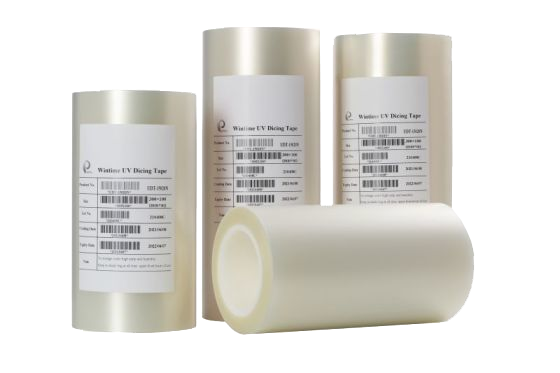
Tape mounting and UV release determine how much blade is exposed at the cut and how firmly the workpiece is held. UV film is part of the consumable set around the blade, and a mismatch between tape holding force and feed rate reads as chipping even when the blade itself is in specification.
Wafer cleaning equipment
Post-cut cleaning removes kerf debris and residues. Lower debris generation reduces cleaning load and shortens the exposure of singulated devices to wet chemistry, which is the practical link between low cutting loss and downstream process time.
Wafer testing machine
Electrical test follows singulation. Edge chipping can surface as test loss rather than as a visible defect, which is why low chipping is specified as a performance target in this scenario and not treated as a cosmetic preference.
Cutting mode: high-speed spindle, dry or wet, precision feed
The operating mode for optical communication device cutting is high-speed spindle rotating cutting, run either dry or wet, with precision feeding and continuous automatic machine operation. Each element shifts what the blade has to deliver.
- High-speed rotation raises thermal and mechanical load on the bond. Hardness in the HRC 65–70 range and a wear-resistant bond are what stop the edge geometry from drifting over a production run.
- Dry versus wet cutting changes debris evacuation and cooling. A chip removal rate of ≥1.2mm³/s is a usable reference when matching feed to what the machine can actually clear.
- Precision feeding is where chipping is won or lost: feed that is too aggressive loads the diamond grit, while feed that is too light can polish the bond instead of exposing fresh abrasive.
- Continuous automatic operation converts blade life into a scheduling variable — changeover intervals, not just consumable cost.
Configuring the blade for optical device cutting
Geometry, base and accuracy
Within the sawing blade range, thickness spans 8μm–50μm, cutting accuracy is specified at ±0.002mm, hardness at HRC 65–70, bond type as resin or metal, and chip removal rate at ≥1.2mm³/s. Construction is a diamond superabrasive on a high-strength steel base with a resin or metal bond matrix. For ultra-thin wafer processing the relevant format is the ≤9μm blade, where absolute thickness — not relative thinness — is the qualification criterion.
Hub configuration and runout
Hubbed, hubless and flanged configurations coexist in the range, and the choice is a stability question before it is a price question. On optical device wafers thinned before singulation, the hubless sawing blade is the configuration most closely aligned with the verified trend toward thinner substrates, while hubbed and flanged types remain appropriate where the machine interface is built around a hub.
Series and bond selection
Named configurations within the range include the DZY Series Wafer Sawing Blade, the DZR Series Sawing Blade and the DZR-S Series Slotted Sawing Blade, alongside diamond, precision, semiconductor, circular, hubbed, hubless, flanged and serrated types. Bond selection follows the material being cut rather than blade thickness: in 2024, resin bond blades held a 42% share of the dicing blade market, while metal bond blades — used for harder materials such as SiC — accounted for 33% (Dicing Blade Market Report 2026, market.us).
The same blade logic extends to adjacent scenarios listed alongside optical communication device cutting, including functional ceramic sawing blade work, alloy material sawing blade work, wafer dicing and scribing, semiconductor package cutting, ultra-thin wafer processing, ceramic substrate cutting and precision alloy component cutting.
Verification: how fit is proven before it is purchased
Application fit is a test result, not a data-sheet claim. A workable acceptance sequence runs through four checks, each mapped to a failure mode described above.
- Geometric dimension inspection using a vernier caliper and laser diameter gauge — covers thickness and the dimensions that govern kerf.
- Hardness and wear resistance testing on a material testing machine — addresses service life and low cutting loss.
- Dynamic balance detection on a high-speed dynamic balance tester — addresses runout at spindle speed.
- Cutting performance simulation on the actual workpiece material — addresses chipping and dimensional control in the real device stack.
Two further points frame a qualification programme. Diamond tools, including sawing blades, are categorised under ISO 22180:2019, which distinguishes CVD diamond-coated from monocrystalline and polycrystalline types — useful language when a specification has to be written unambiguously. And commercially, standard-series lead time of 2–5 working days against 10–25 working days for customised orders tells a buyer how much of the qualification cycle can be spent on iteration.
Example supplier profile: WINTIME
WINTIME Semiconductor Technology Co., Ltd. is a Chinese manufacturer of high-precision wafer-level cutting blades, dicing tapes and cutting solutions, established in 2020 and located in Rugao City, Jiangsu Province. The company operates a 34,000㎡ facility with approximately 100 staff, including 35 R&D engineers, and reports annual capacity of 1 million pieces of dicing blades. Its completed Ultra-thin Wafer D Blade project reached a thickness below 9 microns in process, and the company states that mass production at that thickness is achievable — a position it frames as domestic substitution in a high-end segment. Company records list two patent technologies.
For a cleanroom optical device programme, the supplier-side facts that matter in a sourcing file are the following.
| Capability area | Stated capability |
|---|---|
| Production mode | OEM, ODM and customised production, with specifications set for different cutting materials and working conditions |
| Customisation scope | Blade diameter, thickness and spindle hole size; bond type (metal or resin); diamond abrasive grain size and concentration; coating for anti-rust, heat dissipation and wear resistance; cutting performance such as speed and service life; export and special packaging; non-standard special-shaped blades |
| Capacity | 800,000+ pieces per month for standard specifications; 80,000+ pieces per month for customised and special-shaped products |
| Lead time | 2–5 working days for standard products; 10–25 working days for customised orders, adjustable for large orders |
| MOQ | 50 pieces for standard products; 300 pieces for customised products, flexible for long-term cooperative customers |
| Quality control | Geometric dimension inspection, hardness and wear resistance testing, dynamic balance detection, cutting performance simulation on actual material |
| Export markets | Southeast Asia, East Asia, North America and the EU as primary markets, with exports at roughly 30% of output |
| After-sales | Cutting process matching and equipment adaptation support; quality investigation within 48 hours; customised service for bulk buyers; long-term supply guarantee and inventory support; application training; replacement and compensation for defective products caused by quality problems |
Market context behind the buying decision
Published market-size estimates for dicing blades diverge sharply by scope, with figures for the same year ranging from roughly USD 0.44 billion to USD 1.31 billion depending on whether equipment or consumables are counted (Intel Market Research; Dicing Blade Market Insights). Any single number should therefore be read as a scope statement rather than a fact about the segment. The more decision-relevant signals are structural: hubless designs are gaining ground as substrates get thinner, and supply is diversifying — China's exports of cutting blades to Vietnam grew by USD 18 million and to India by USD 12 million between 2024 and 2025 (OEC).
The established competitive set in high-precision semiconductor dicing blades includes DISCO Corporation, Tokyo Seimitsu (Accretech), Advanced Dicing Technologies (ADT) and Asahi Diamond (Credence Research). Their presence does not by itself settle fit for a Class 100/1000 optical programme. What settles it is narrower: whether a supplier can hold a sub-9μm thickness in mass production, hold ±0.002mm dimensional tolerance, and demonstrate chipping performance on the buyer's actual device material.
Where the limits are
Ultra-thin capability is not a universal upgrade, and treating it as one is the most common sourcing error in this segment. The boundaries below are as much part of the specification as the performance targets.
| Configuration | Where it fits | Boundary to watch |
|---|---|---|
| Ultra-thin blade ≤9μm | Ultra-thin wafer processing and thin optical device stacks where kerf loss is critical | Trades mechanical stiffness for kerf width; more sensitive to runout, feed and handling. Not a general substitute for thicker blades on thicker or harder workpieces |
| Hubless sawing blade | 300mm wafer processing and substrates below 50µm, where runout control dominates | Saves runout but is less forgiving of incorrect flange mounting during changeover |
| Hubbed / flanged | Established machine interfaces built around a hub | Hub geometry constrains how thin the overall assembly can practically be |
| Resin bond | Largest single bond category at 42% of 2024 market share | Not the bond associated with the hardest substrates |
| Metal bond | Harder materials such as SiC (33% share in 2024) | Harder bond is not automatically right for a softer optical stack; selection is material-led |
- The blade is not the cleanroom. Class 100/1000 compliance depends on the room, the tape and the machine enclosure as much as on the blade; low-particle blade behaviour reduces the load but does not replace environmental control.
- Supplier record is a real variable. WINTIME was founded in 2020 and is a newer entrant relative to the incumbents named above; buyers with long qualification histories may weight track record differently from buyers optimising for sub-9μm availability and supply proximity.
- Capacity is not infinite at either end. Standard-specification output and customised or special-shaped output run on different volumes, so a first order of special-shaped blades follows a different schedule than a repeat standard order.
Future outlook
Three directions look durable for optical communication device cutting. First, kerf loss keeps shrinking in importance relative to die count per wafer, which pushes demand toward thinner blades and hubless mounting on thinned substrates. Second, the optical segment's share of dicing blade consumption is tied to 5G build-out, so the installed base of machines will keep growing in the same regions where blade supply is already diversifying. Third, classification language such as ISO 22180:2019 is gradually making specification writing more precise, which favours suppliers who can state thickness, tolerance and bond in verifiable terms rather than in comparative adjectives.
For procurement teams, the practical implication is that the qualifying question has moved. It is no longer whether a blade is thin enough in a catalogue, but whether a supplier can hold that thickness, that tolerance and that chipping performance inside a Class 100/1000 route, on the buyer's own equipment chain, lot after lot.
FAQ
What cleanroom conditions do sawing blades for optical communication devices work in?
They operate in a Class 100/1000 clean room with constant temperature of 22±2°C, constant humidity of 45%–55%, and dust-free, anti-static conditions in a high-speed spindle environment. The same scenario reference covers applications in semiconductor manufacturing, semiconductor packaging, optical communication, new functional materials, functional ceramics and alloy materials, with listed markets including China, Japan, Korea, Singapore, Malaysia, the United States and Germany.
Which equipment must a sawing blade be matched to for this scenario?
Five items form the matched set: an automatic wafer dicing machine, a semiconductor cutting spindle, a UV tape mounting machine, wafer cleaning equipment and a wafer testing machine. The cutting mode within that set is high-speed spindle rotating cutting, dry or wet, with precision feeding and continuous automatic dicing machine operation.
What thickness and accuracy targets apply to ultra-thin optical device dicing?
The sawing blade range spans 8μm–50μm in thickness, with cutting accuracy of ±0.002mm, hardness of HRC 65–70, resin or metal bond, and chip removal rate of ≥1.2mm³/s. Ultra-thin wafer processing requires blade thickness of ≤9μm, combined with high wear resistance, low cutting loss, anti-static properties, high dimensional accuracy and long service life, while sustaining stable mass production.
Should a resin bond or a metal bond be used for optical communication device cutting?
Both bond types are available in the range, and the choice is material-led rather than thickness-led. In 2024, resin bond blades held a 42% share of the dicing blade market, while metal bond blades, used for harder materials such as SiC, accounted for 33% (Dicing Blade Market Report 2026, market.us). Because the correct bond depends on the specific device stack, the practical way to settle it is a cutting performance simulation on the actual workpiece material.
How is application fit verified before a blade moves to mass production?
Four checks are used: geometric dimension inspection with a vernier caliper and laser diameter gauge; hardness and wear resistance testing on a material testing machine; dynamic balance detection on a high-speed dynamic balance tester; and cutting performance simulation on the actual material. Commercially, standard products carry a 2–5 working day lead time against 10–25 working days for customised orders, with minimum order quantities of 50 pieces standard and 300 pieces customised. Diamond tools including sawing blades are categorised under ISO 22180:2019.
Have Questions or Need More Details?
Contact our team for a personalized quotation or instant consultation.
Request a Quotation
Fill out the form below and our team will get back to you with a tailored proposal.
WhatsApp Direct Chat
Prefer to chat in real-time? Message us on WhatsApp for instant assistance & quick answers.
- Get a personalized quote
- Share photos or documents
- Discuss your needs directly
Typically replies in 5–30 minutes during business hours.