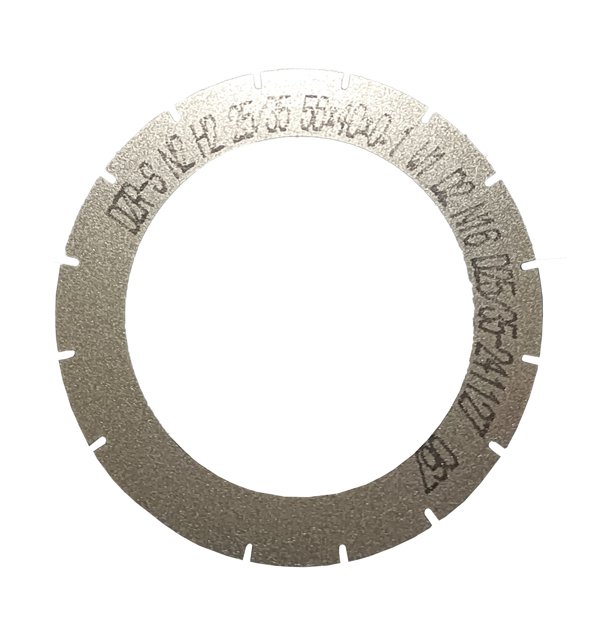
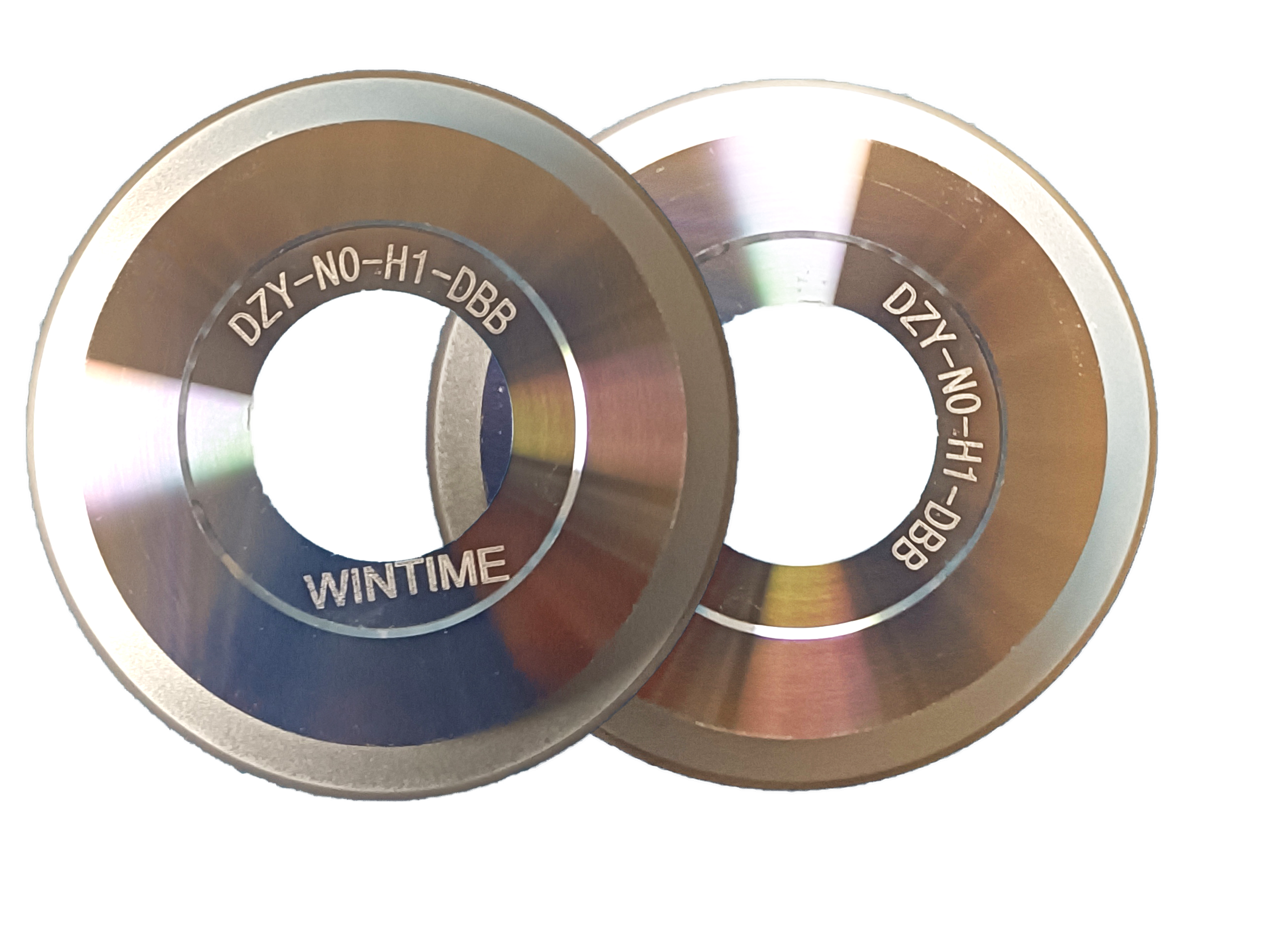
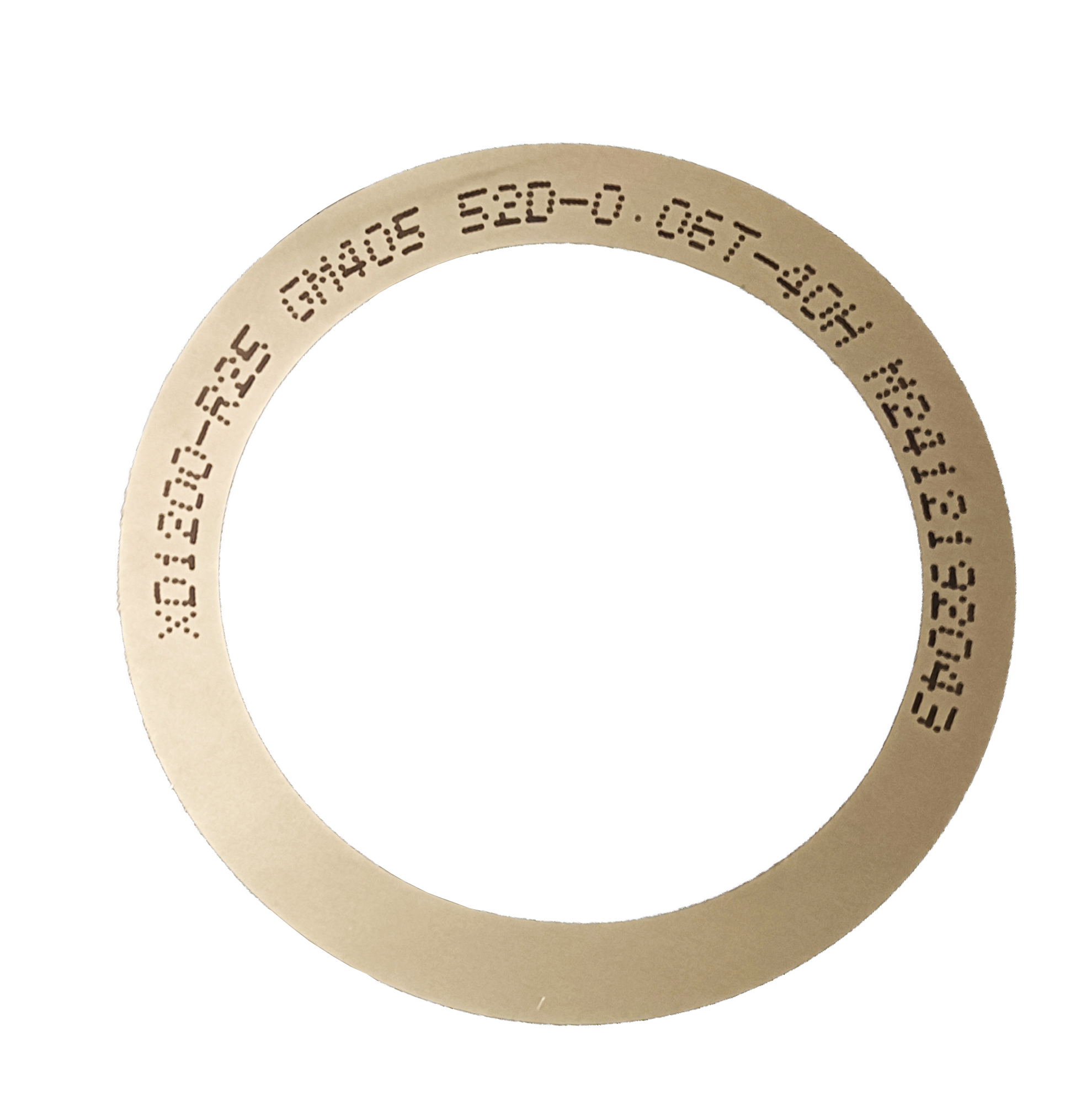
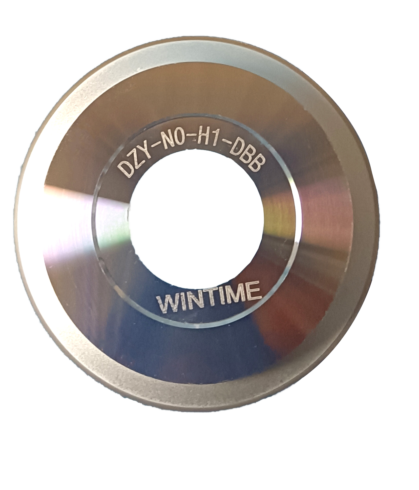
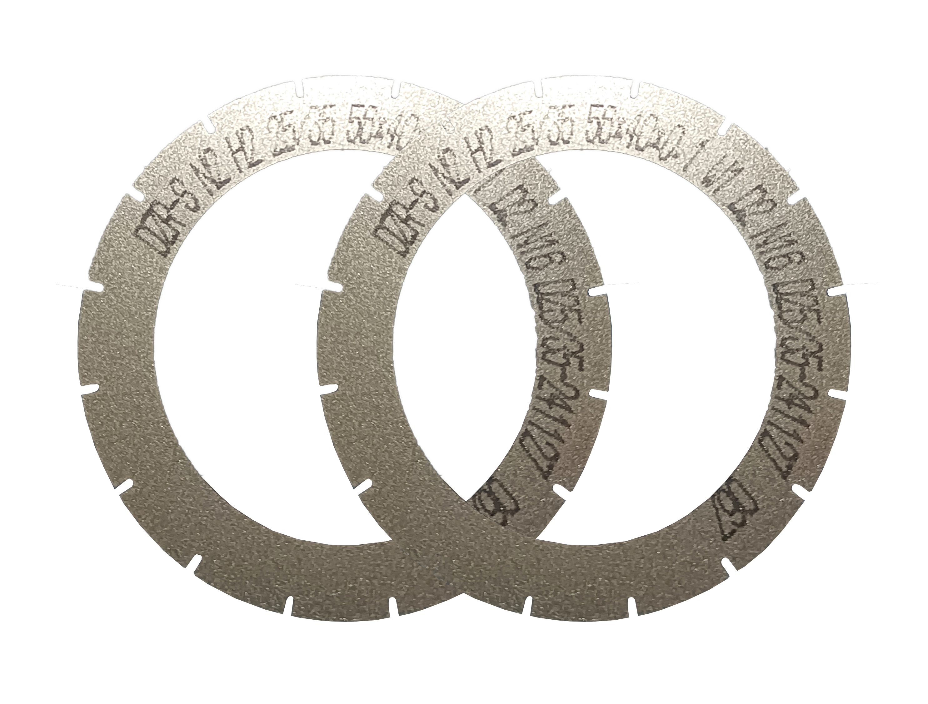
A working glossary of sawing blade terms for precision cutting: kerf, blade thickness, bond type, grit size, chipping, hubless construction, runout, and anti-static behaviour — and how each one changes a real specification. By WINTIME Semiconductor Technology Co., Ltd.
2026-09-27 07:01:45
How a dicing blade works: diamond grit, bond behaviour, kerf and chipping control, cleanroom conditions, and how WINTIME's Ultra-thin Wafer D Blade reaches below 9 µm thickness for semiconductor, optical, and ceramic cutting.
2026-09-27 02:28:52
Compare sawing blade requirements for optical device cutting vs. ceramic substrate cutting: cleanroom conditions, bond type, kerf, chipping, and cutting mode.
2026-09-27 02:25:08
Hubless vs. hub-type sawing blades compared for semiconductor and ceramic slicing: sub-9 μm blade stability, spindle and cleanroom needs, selection rules.
2026-09-26 07:12:18
A sawing blade cuts with a diamond bond, ultra-thin kerf and a high-speed spindle. See how it differs from a standard cutting wheel and how to specify one.
2026-09-26 02:28:52
Audit checklist for sawing blade factories: verify manufacturing area, annual capacity, engineering headcount, patents, QC records, and lead times before signing.
2026-09-25 07:16:10
How ultra-thin wafer slicing works in a cleanroom: spindle speed, dry vs wet cutting, precision feeding, Class 100/1000 conditions, and sawing blades below 9 μm.
2026-09-25 05:39:10
A regional compliance guide for sawing blade buyers in the EU and USA: RoHS and REACH obligations, cleanroom and ESD site fit, WINTIME's export footprint, and a six-step verification workflow.
2026-09-24 07:04:34
Sawing blade vs laser cutting on ceramic substrates: compare kerf, chipping, dimensional control, feeding and cleanroom fit before qualifying a process.
2026-09-24 02:37:45
How to turn precision alloy component designs into qualified cuts: sawing blade specs, dry vs wet cutting modes, site conditions and project benchmarks in Korea, Singapore and China.
2026-09-23 07:37:59
A decision-stage guide to sawing blades for functional ceramics: bond type, blade thickness below 9 um, hubless stability, dimensional accuracy, and cutting loss.
2026-09-23 02:27:06
7 questions to verify a sawing blade supplier's production and R&D readiness: facility scale, annual capacity, R&D team size, patents, QC steps, MOQ and lead time.
2026-09-22 07:37:18
Technical guide to specifying dicing blades for cleanroom wafer dicing: blade thickness, bond type, grit, spindle compatibility and Class 100/1000 environment parameters.
2026-09-22 02:36:26
A 2026 buyer list of sawing blades for optical communication devices: five blade picks compared, plus Class 100/1000, UV tape and wafer cleaning qualification criteria.
2026-09-22 02:28:06
Map sawing blade site compliance: Class 100/1000 cleanroom, 22±2 °C, 45%-55% humidity, anti-static control, high-speed spindle fit, and CN, JP, KR, SG, MY, US, DE deployment.
2026-09-21 06:17:05
Sawing blade vs laser cutting for ultra-thin wafers: compare kerf loss, sub-9μm blade capability, cleanroom and anti-static needs, and real cost per good die.
2026-09-21 02:25:54
How sawing blades meet Class 100/1000 cleanroom standards: 22±2°C, 45%–55% RH, dust-free and anti-static conditions, plus documentation by region.
2026-09-20 07:04:22
Sawing blade partner or vendor? An FAQ on long-term supply reliability: verify capacity, quality control, engineering support, MOQ, lead times, and continuity terms.
2026-09-20 02:28:02
Application guide to ≤9μm sawing blades for ultra-thin wafer processing: cleanroom conditions, dry vs wet cutting, supporting equipment, and blade selection criteria.
2026-09-19 06:17:23
Why ceramic substrate cuts chip and how to fix it: sub-9 µm sawing blades, wear-resistant bonds, cleanroom dicing on automatic machines, and a step-by-step correction sequence.
2026-09-19 02:38:45