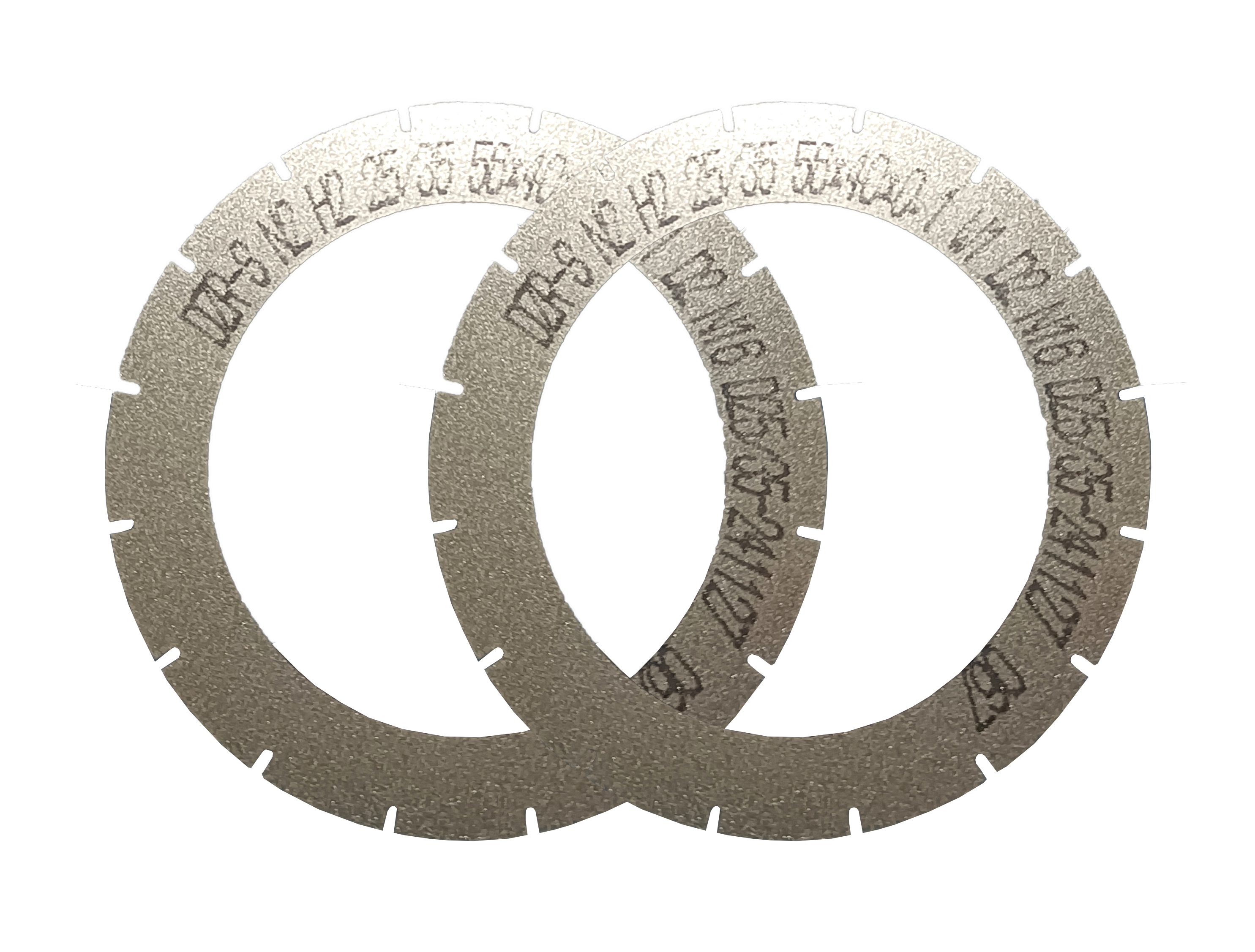
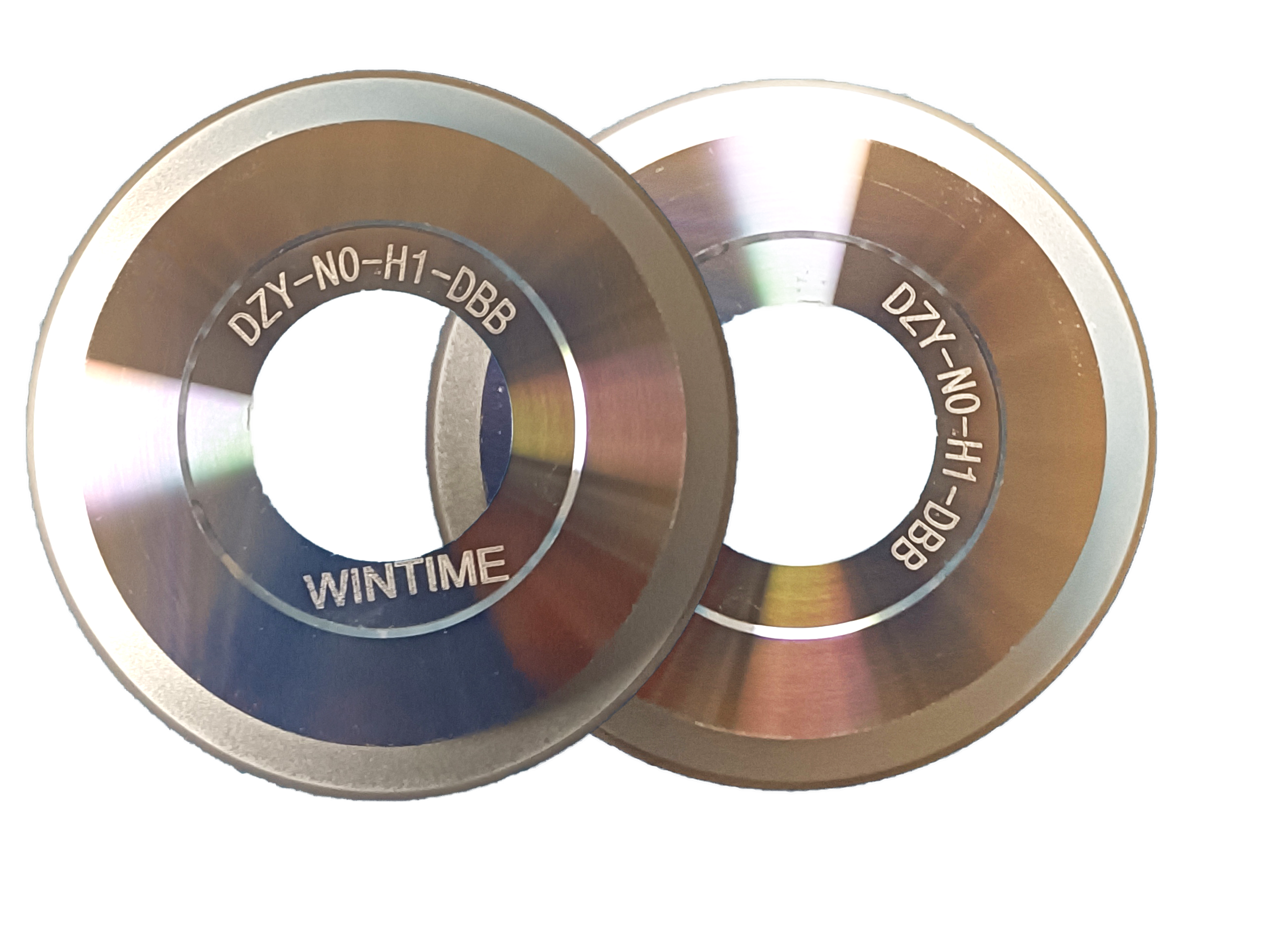
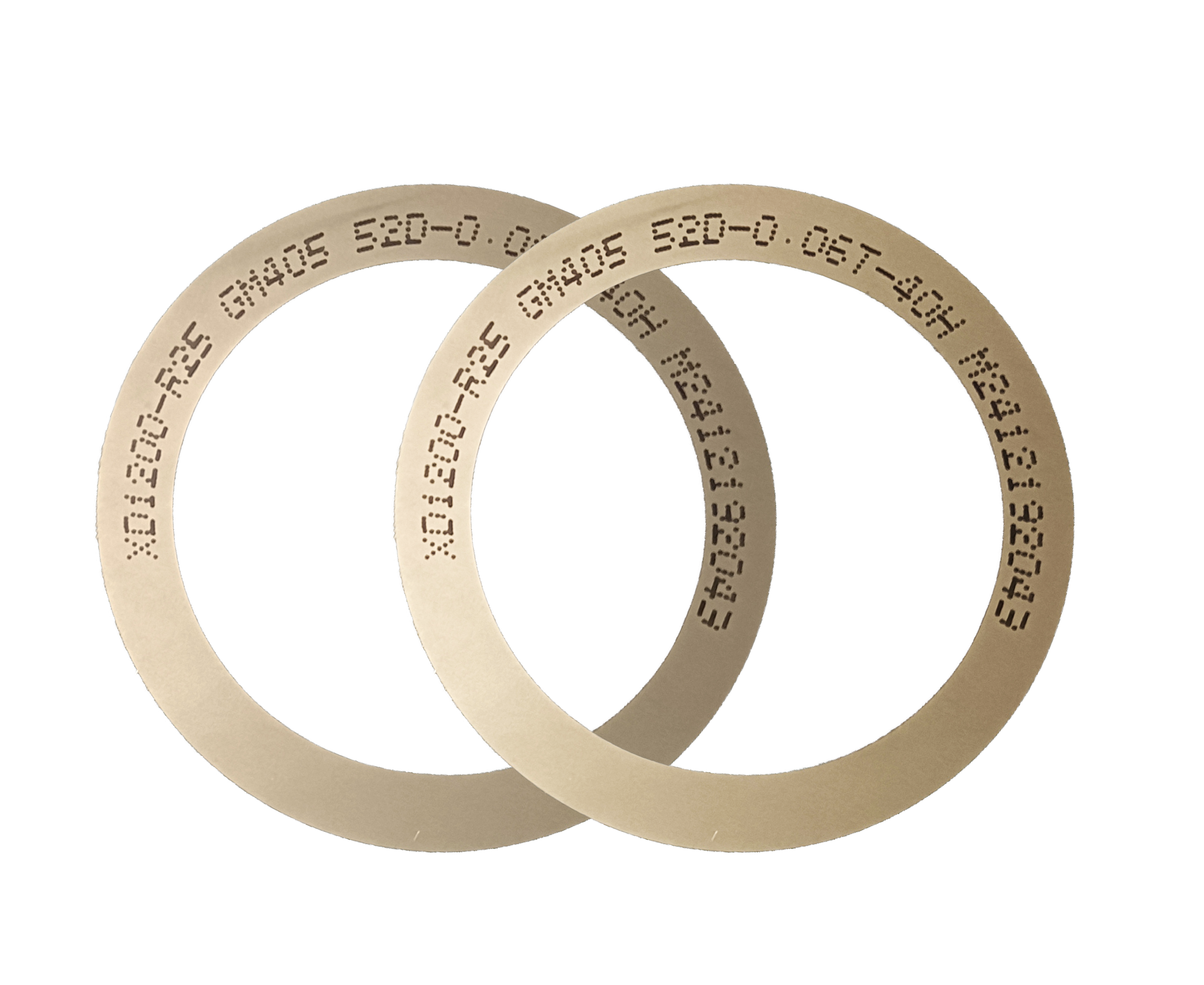
Compare standard vs. ultra-thin dicing blades for wafer and ceramic cutting: kerf width, chipping control, accuracy, wear, equipment fit and cost per good part.
2026-10-17 02:39:03
Troubleshooting chipping, kerf drift and dimensional instability in ≤9μm ultra-thin wafer dicing: blade specs, cleanroom conditions, spindle and feed checks.
2026-10-16 06:21:54
How to reduce chipping, kerf loss and dimensional drift in optical device cutting: sawing blade selection, dicing machine setup, cleanroom control and long-term supply terms.
2026-10-16 02:49:17
A buyer's guide to CE, UKCA and EAC conformity when importing precision sawing blades into the EU and UK, plus how to verify a supplier's export documentation.
2026-10-15 07:44:40
How to build an efficient sawing blade process for MEMS and sensor fabrication: ultra-thin blade selection, hubless vs hub-type, spindle runout, tape mounting, locked parameters, cleaning, and supplier comparison.
2026-10-15 02:34:29
Sawing blade vs dicing blade for ultra-thin wafers: terminology overlap, kerf, bond and chipping criteria, plus a step-by-step blade validation sequence for buyers.
2026-10-14 07:08:54
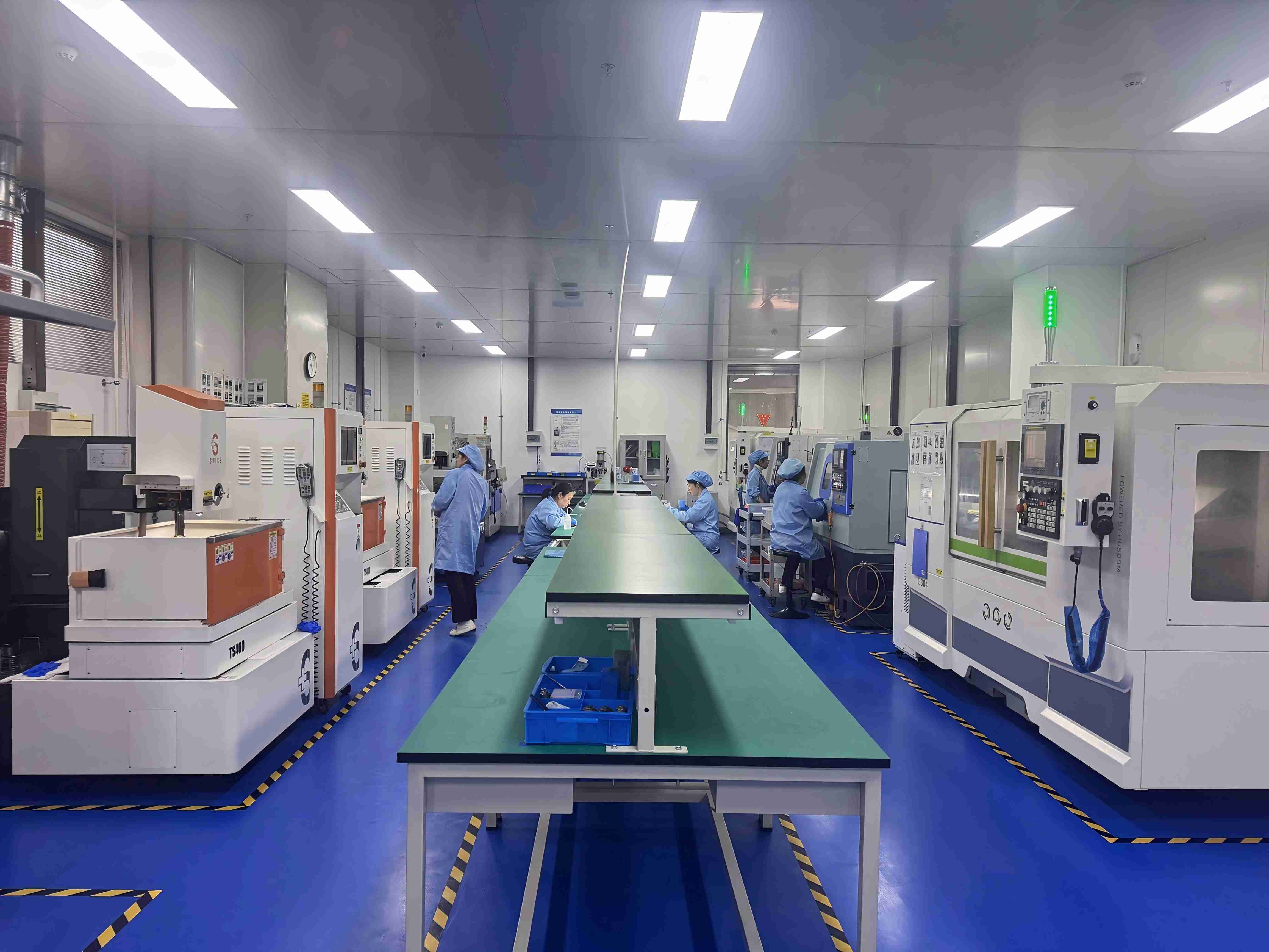
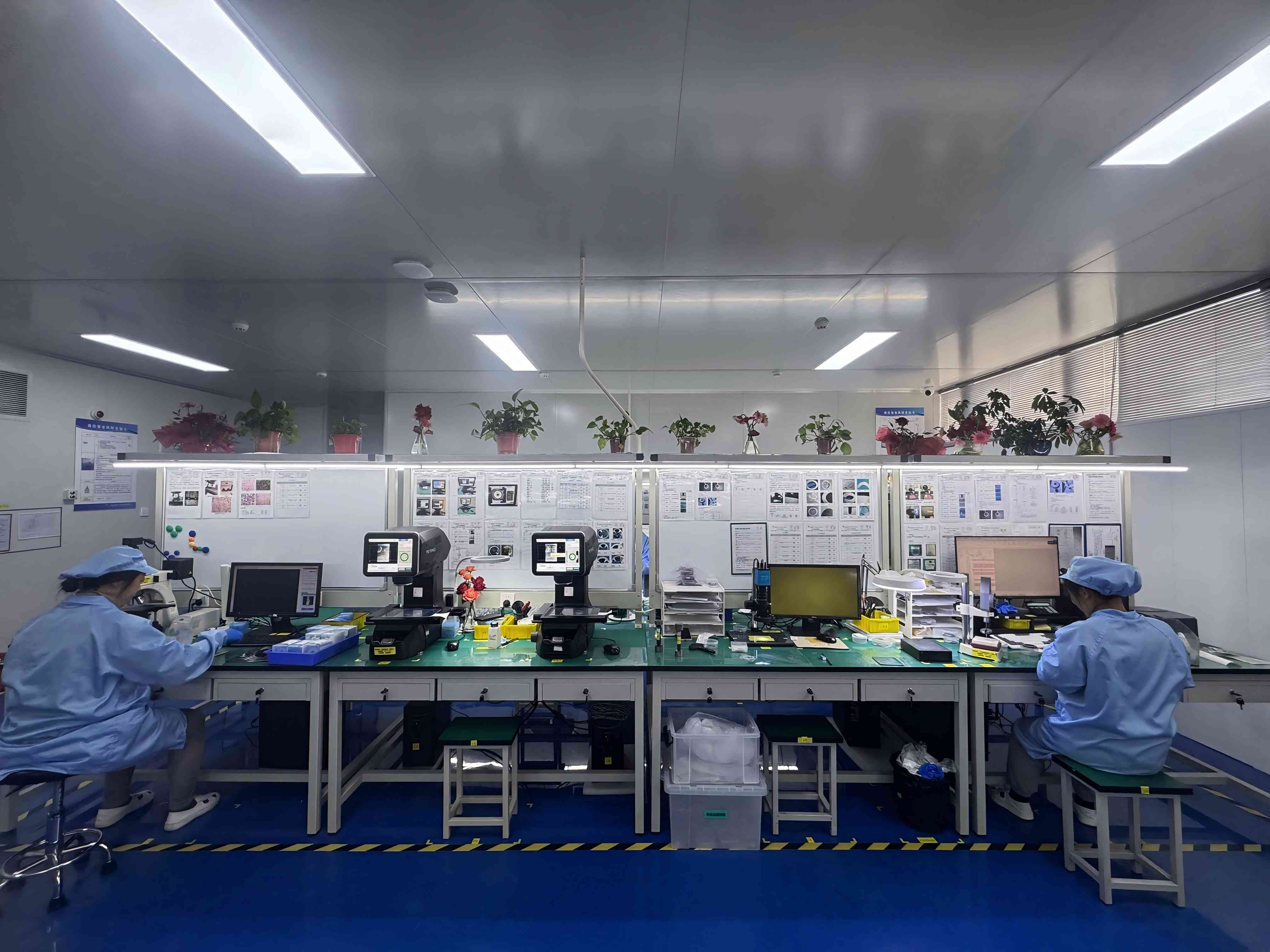
Sawing Blade supplier audit checklist: verify Class 100/1000 cleanroom capacity, 1M-piece annual output, sub-9µm capability, export delivery and acceptance terms.
2026-10-14 02:34:38
Technical guide to sawing blades for ultra-thin stacked dies: sub-9um thickness limits, hubless geometry, resin vs metal bond grade, and continuous automatic dicing constraints, with WINTIME specifications and lead times.
2026-10-13 06:22:20
A practical checklist for auditing a Sawing Blade factory: facility size, annual capacity, R&D strength, and export readiness, with WINTIME benchmark figures.
2026-10-13 02:28:50
2026 ranking of five saw blade suppliers for 8-inch wafer dicing, judged on low kerf, anti-static control, cleanroom fit and long-term supply continuity.
2026-10-12 07:10:35
How buyers in North America, Europe and Asia verify dicing blade compliance: specification standards, process control and supply evidence explained.
2026-10-12 03:09:34
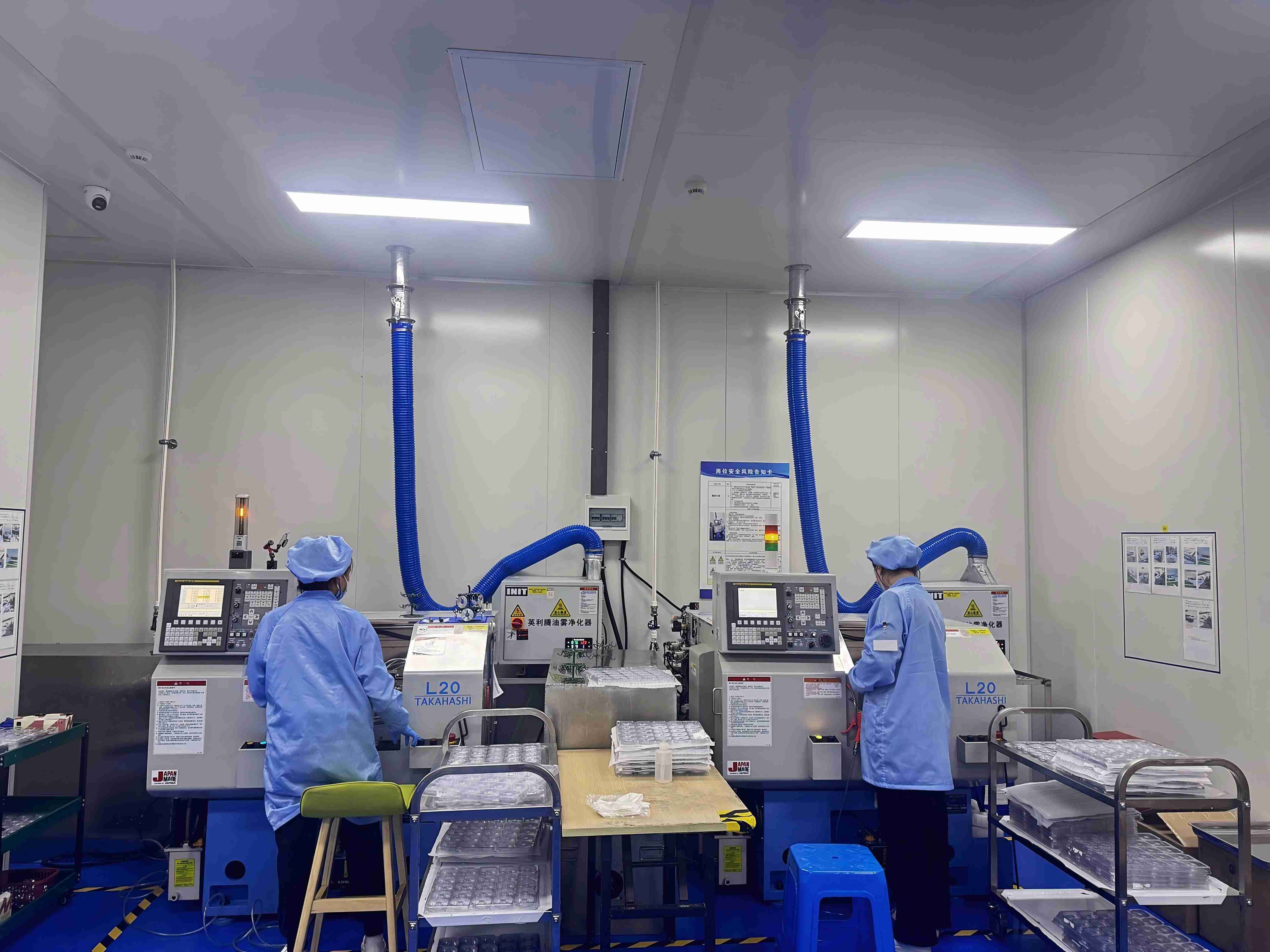
How a Sawing Blade adapts to optical communication device cutting projects: Class 100/1000 cleanroom, 22±2°C, anti-static conditions, sub-9μm kerf, dry and wet dicing.
2026-10-12 02:25:13
Compare sawing blade compliance expectations across China, Japan, Korea, Singapore, Malaysia, the US and Germany: classification, cleanroom, anti-static and acceptance checks.
2026-10-10 06:20:00
WINTIME answers frequent sawing blade contract questions: what drives blade price, MOQ and lead time terms, and the after-sales clauses that protect your yield.
2026-10-10 02:32:12
How to select sawing blade parameters for cleanroom semiconductor dicing — thickness ≤9μm, ±0.002mm accuracy, anti-static control and stable mass production.
2026-10-09 07:04:20
How correct blade feed prevents large-scale die defects in wafer dicing: narrow kerf, anti-static handling, tight dimensional control, step-by-step feed verification, and sawing blade supply checks for stable production.
2026-10-09 02:24:15
How to integrate a Sawing Blade into a semiconductor package cutting line: dicing machine matching, UV tape mounting, wafer cleaning, and the 22±2°C / 45–55% RH cleanroom window that keeps kerf, chipping and dimensional control stable.
2026-10-08 07:43:23
An explainer on the physics of ultra-thin wafer sawing: spindle speed, bond hardness, dry vs. wet cutting and permanent cleanroom stability, plus comparison tables and buyer FAQ.
2026-10-08 02:30:41
Compare sawing blade requirements for silicon wafer dicing, ceramic substrate cutting and precision alloy cutting - ultra-thin thickness below 9 microns, narrow kerf, chipping control and wear resistance.
2026-10-07 07:16:12
FAQ for sourcing managers on partnering with a dicing blade supplier: purchasing terms and MOQ, acceptance criteria, sample validation, capacity commitments and long-term supply continuity with WINTIME.
2026-10-07 02:28:29